

The first four sections of this piece explain the terminology and architecture for readers who are new to NVIDIA’s rack systems. If you’re here for the SemiAnalysis Kyber delay controversy, feel free to jump straight to Section 5.
NVIDIA headlines these days mention rack names more often than chip names. Just this past weekend, a SemiAnalysis claim that a rack called Kyber had slipped by more than a year collided with NVIDIA’s rebuttal that its roadmap is intact, and the related stocks swung on it within a single day.
The trouble is that reading this kind of news requires knowing far too many names just to parse a single sentence. What is Rubin? What is Kyber? Why did NVL144 suddenly become NVL72? And when is Feynman supposed to arrive?
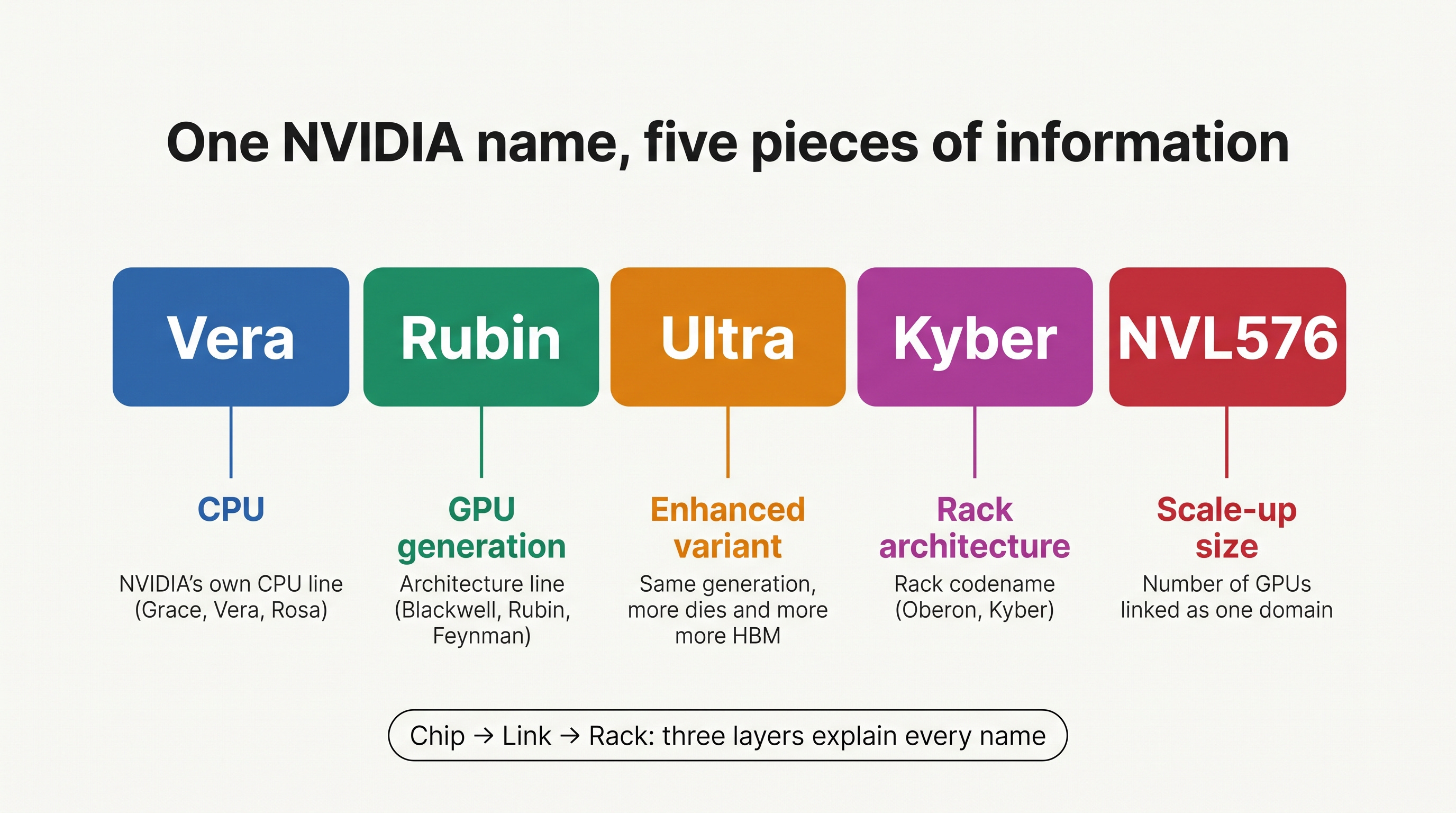
The confusion is entirely reasonable. A name like Vera Rubin Ultra Kyber NVL576 packs five separate pieces of information into one string: the CPU, the GPU, the generation, the rack architecture, and the scale of the interconnect.
It looks complicated, but these names sort neatly into three layers: chip, link, and rack. Start at the bottom with the chip and work your way up one layer at a time, and the naming maze turns out to run on surprisingly simple rules.
Once you have those rules in hand, you can take the SemiAnalysis claims that shook the market and pick them apart sentence by sentence. I’ll say this up front: I believe those claims planted far more fear in the market than what they actually said. The rest of this piece walks through why, one piece of evidence at a time.
Table of Contents
The chip layer: the logic behind the names
The link layer: NVLink and scale-up
The rack layer: Oberon, the present
Kyber: the problem the next rack has to solve
Reading the sentences closely
So is midplane yield actually a problem?
The figures in this piece are based on public sources; the interpretations and outlook are my own analysis. Nothing here is a recommendation to buy or sell any security. Roadmaps and specifications reflect announced plans and may change.
1. The chip layer: the logic behind the names
NVIDIA ships a new GPU architecture every year. An architecture is the chip’s underlying design, and a single architecture spawns multiple products, from data center parts to workstation cards.
The generation selling today is Blackwell. The one ramping in the second half of this year is Rubin, and the one arriving in 2028 is Feynman. All of them are named after scientists: Blackwell for the mathematician David Blackwell, Rubin for the astronomer Vera Rubin, and Feynman for the physicist Richard Feynman.
Separately from its GPUs, NVIDIA also builds its own CPUs, which sit next to the GPU and handle data preparation and orchestration. These follow their own naming lineage, Grace, Vera, Rosa, all named after women scientists.
So when the news says Vera Rubin, it isn’t referring to a single chip. It’s a platform name that bundles a CPU called Vera with a GPU called Rubin.
The origin of this naming scheme is a fun bit of trivia. The previous generation, Grace Hopper, split one computer scientist’s name in two: Grace for the CPU, Hopper for the GPU. Vera Rubin does the same with one astronomer’s name.
Starting with the next generation, Rosa Feynman, the pairing shifts to two different scientists, the Nobel-winning medical physicist Rosalyn Yalow and the physicist Richard Feynman. But the rule itself survives: the CPU name comes first, the GPU name second. Know that rule and you can decode any codename on sight, even one you’ve never seen before.
Finally, there’s Ultra. Ultra is not a new architecture. It’s a beefed-up version of the same generation, and what gets beefed up is the number of dies in a package.
A die is the actual silicon chip. Because there are physical limits to how large a single die can grow, the industry now places multiple dies side by side on one substrate and packages them as a single giant chip. Rubin uses two dies per package.
Rubin Ultra adds more dies and also increases the HBM (High Bandwidth Memory), the high-speed memory stacked right next to the GPU. In AI workloads, how fast the GPU can be fed data determines performance, so HBM capacity and bandwidth effectively set the ceiling on what the chip can do.
To sum up, the chip layer has three kinds of names: the GPU generation (Rubin, Feynman), the CPU generation (Vera, Rosa), and the enhanced-variant marker (Ultra). But today’s AI models have grown too large for any single GPU to handle, no matter how good. The real competition is happening one layer up, in how many of these chips you can bind together to act as one.
2. The link layer: NVLink and scale-up
Training or serving a large language model takes dozens or hundreds of GPUs. The catch is that these GPUs don’t work independently.
A single model is sharded across many GPUs, so they constantly exchange intermediate results mid-computation. If that communication is slow, even the most expensive GPUs end up idle, waiting on data. How fast and how widely you can bind GPUs together determines the performance of the whole system.
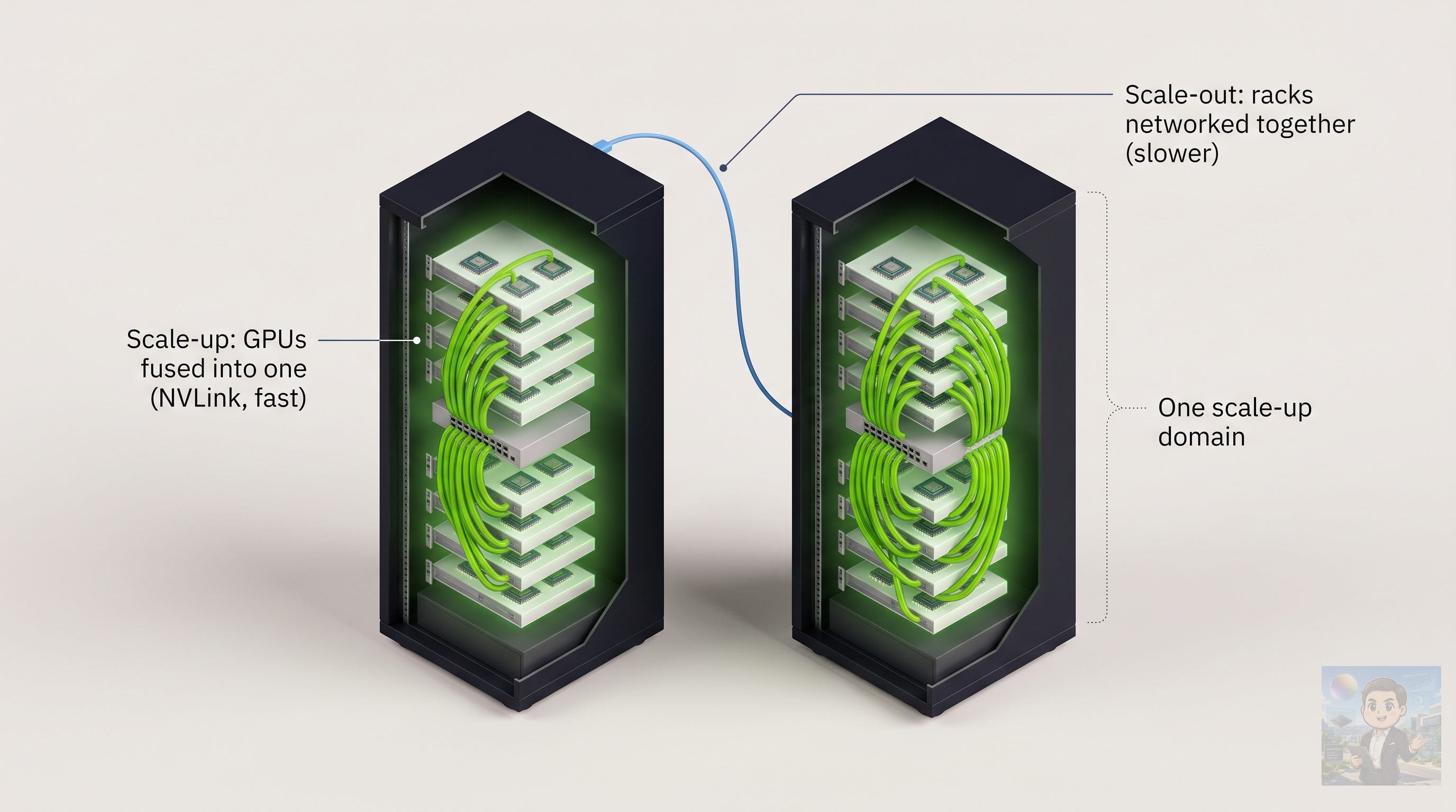
There are two ways to connect them. In the current generation, wiring GPUs together inside a single rack over ultra-fast dedicated links, so they effectively behave as one giant GPU, is called scale-up. Stitching those racks together over a conventional network to grow the overall cluster is called scale-out.
For the same data, scale-up traffic inside a rack is far faster and lower latency than scale-out traffic between racks. So the basic recipe is to pack the chattiest GPUs into one rack, then network those racks together to reach data center scale.
NVIDIA’s scale-up technology is NVLink, a dedicated pathway that connects GPU to GPU far faster and with far less latency than a regular network. GPUs bound by NVLink can read and write each other’s memory as if it were their own.
The chip that ties all of these GPUs together, acting as a switchboard, is NVSwitch. NVSwitch belongs to the scale-up side along with NVLink, sitting among the GPUs inside a rack so that any GPU can talk directly to every other GPU. The set of GPUs that moves as one body this way is called a scale-up domain.
Scale-out, the rack-to-rack connection, is handled by separate networking gear. NVIDIA offers two options there: InfiniBand and the Ethernet-based Spectrum-X.
NVL is short for NVLink, and the number after it is the count of GPUs bound into a single scale-up domain. NVL72 means a system where 72 GPUs move as one. The bigger the number, the larger the model you can run without hitting communication bottlenecks.
There’s one source of confusion: the counting convention changed midstream. The first Rubin rack was originally announced as NVL144. With two dies per GPU package, NVIDIA counted 144 dies across 72 packages and called it 144.
It then reverted to counting packages, for naming consistency with the prior generation’s GB200 NVL72, and the rack was finalized as VR200 NVL72. VR200 is the successor to the GB200 numbering: just as GB200 stood for the Grace CPU plus Blackwell GPU combination, VR200 stands for Vera plus Rubin. So the NVL144 in last year’s articles and the VR200 NVL72 in this year’s articles are the same machine.
3. The rack layer: Oberon, the present
The rack, which kept showing up above as the boundary of scale-up, is the third layer. A rack, using GB200 NVL72 as the reference, is a cabinet 0.6 meters wide, about 1.1 meters deep, and about 2.2 meters tall, weighing in at 1.4 tons, with trays of GPUs slotted in one on top of another.
NVIDIA gives its racks their own codenames too. The rack in service since the GB200 generation, carrying through to this year’s Rubin, is Oberon.
In Oberon, compute trays carrying GPUs and CPUs slot in horizontally, layer by layer, with switch trays carrying NVSwitch chips in between. At the back, bundles of copper cables connect every tray’s GPUs to the NVSwitches.
The heat is intense enough that the rack is liquid-cooled rather than air-cooled. In the VR200 NVL72 configuration, one rack holds 72 GPU packages and 36 Vera CPUs.
Copper is the cheapest and most proven way to wire GPUs together. Its weakness is distance. The longer the wire, the more the signal degrades, at which point you either add amplifiers or switch to optics.
Optics requires converting electrical signals to light and back again, and the transceivers doing that conversion burn double-digit watts per port. That’s a cost copper simply doesn’t have, since electricity flows through it directly.
So the GPUs you want to fuse into one body over NVLink need to sit within copper’s reach, which means packing them as close together as possible inside a single rack. That’s why 72 GPUs get crammed into one cabinet, and it’s also why the physical size of the rack caps the size of the scale-up domain.
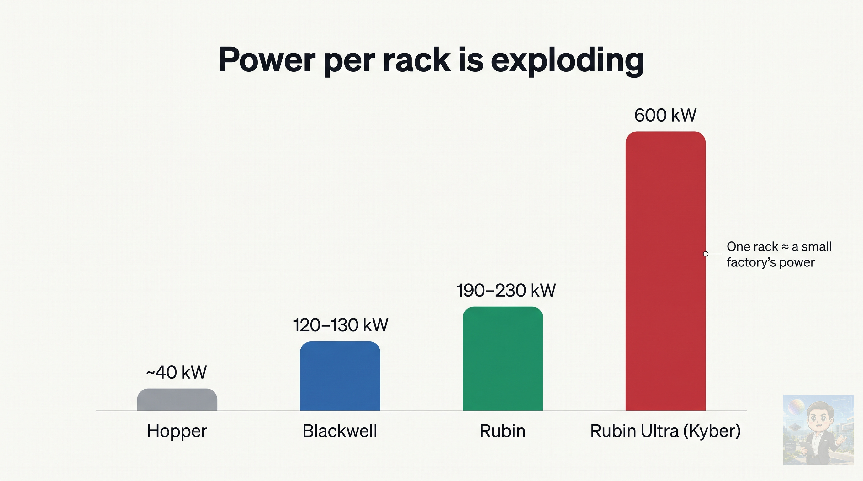
Copper saves power on the wiring, but the power the GPUs themselves draw stacks up with density. With 72 GPUs each pushing past 1 kW packed into one cabinet, per-rack power has climbed from roughly 40 kW in the Hopper generation to 120-130 kW for Blackwell and 190-230 kW for Rubin.
A single rack now draws as much electricity as a small factory. At that point the rack becomes the anchor around which a data center’s entire power and cooling design is built. And the next rack triples that number.
4. Kyber: the problem the next rack has to solve
Kyber is the new rack debuting alongside Rubin Ultra in the second half of 2027. The goal is simple to state: where Oberon slots its trays horizontally, Kyber stands its compute trays vertically to push density higher, fitting 144 GPU packages in one rack. That’s exactly double Oberon, and per-rack power surges to the 600 kW class.
In the Rubin Ultra generation, Kyber is slated to come in three configurations: NVL72, NVL144, and the flagship NVL576, which binds the GPUs of multiple racks into a single NVLink domain.
What separates scale-up from scale-out isn’t the physical boundary of the rack itself but whether the GPUs are fused into one body over NVLink. Multiple racks joined by NVLink still count as one scale-up domain. The Blackwell generation actually deployed exactly that: GB200 NVL36x2, which linked two racks with copper cables so that 72 GPUs split across them formed a single NVLink domain.
But copper’s practical reach ends at the adjacent rack, which is why scale-up has so far stayed within one or two racks. NVL576 is the first configuration to push that boundary out to a multi-rack scale.
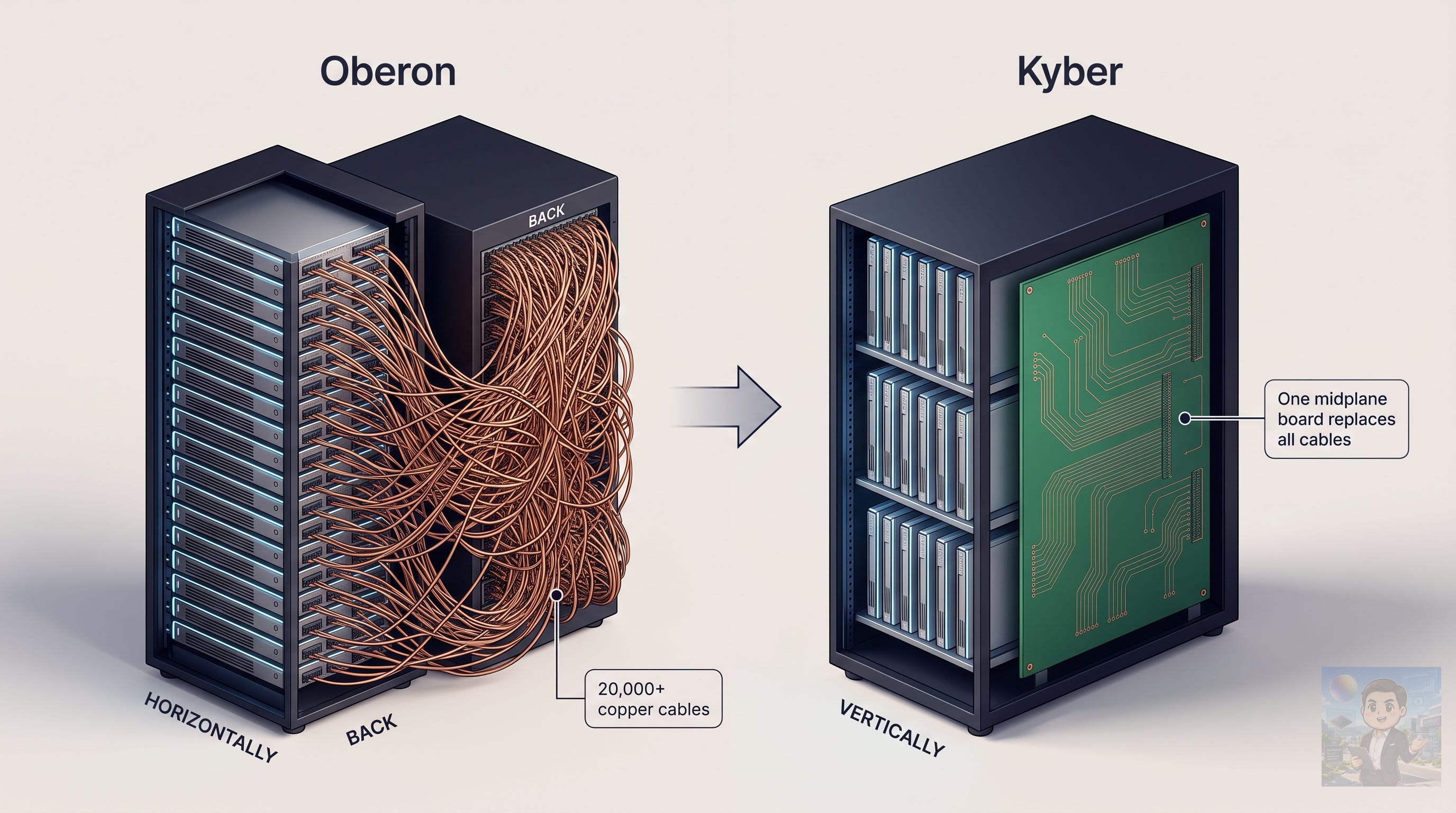
The key question is what connects those 144 GPUs. One analysis puts the copper cable count at over 20,000 if you wire it the Oberon way. Assembly, repair, and reliability management all turn into a nightmare.
NVIDIA’s answer is a midplane: one enormous circuit board. Everything those 20,000 cables did gets replaced by traces printed on the board, and the trays plug directly into it. It’s a design that eliminates the cable harness outright.
But building it is another matter. According to industry analysis, the board laminates three 26-layer boards into a 78-layer stack nearly one square meter in area, with trace spacing at or below 25 micrometers, while holding electrical characteristics within a 5 percent tolerance so the ultra-high-speed signals don’t smear.
More layers kill the signal. A bigger panel means one defect anywhere scraps the whole thing, dragging down yield. The heart of the rack is no longer the GPU. It’s this one board.
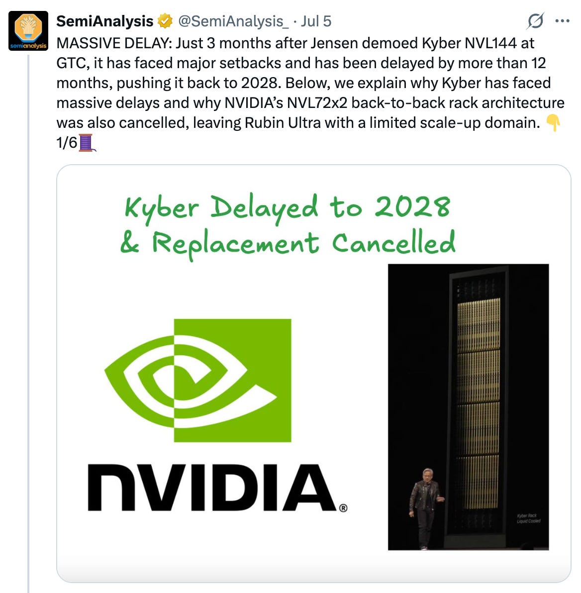
The recent delay controversy erupted at exactly this point.
SemiAnalysis made four claims.
Kyber NVL144 has slipped to 2028 over the manufacturability of this midplane.
NVL576, which binds multiple racks with optics, may also be delayed or limited to small volumes.
NVL72x2, the stopgap that would have doubled scale-up by placing two Oberon racks back to back over copper, was cancelled after pushback from cloud providers.
And the four-die Rubin Ultra was cancelled, leaving only the two-die version.
All four claims live in the layers we just covered: board manufacturability, optical scale-up, copper’s distance limit, and dies per package.
NVIDIA immediately pushed back, saying its roadmap is intact.
5. Reading the sentences closely
NVIDIA’s rebuttal was one sentence: “Our roadmap is intact.”
It did not respond point by point to the specific claims about midplane yield or the NVL72x2 cancellation. So I went the other way and read the SemiAnalysis claims themselves, sentence by sentence.
Let me say this up front.
The problem with these claims is not that every sentence is false.
Each sentence is written so it can be walked back no matter how things turn out, while the overall framing makes it read as if the entire Rubin Ultra generation is wobbling.
That gap, planting far more fear in the market than what was actually said, is the problem.
Start with their headline.
It opens loud: “MASSIVE DELAY” and “delayed by more than 12 months, pushing it back to 2028.”
But Kyber’s official schedule is the second half of 2027, so a delay of more than 12 months means late 2028 at the earliest. Slipping from the second half of 2027 into early 2028 and slipping by more than 12 months, into late 2028 or, taken literally, 2029, are enormously different outcomes. Yet they blur the two together, framing the headline as if something catastrophic has happened to NVIDIA.
Next, the NVL576 sentence: “likely delayed or restricted to small volumes.” That hangs two options off a word of estimation. If it ships on time but in small volume, they’re right. If it ships late, they’re also right.
For this sentence to be wrong, a flagship top-end configuration would have to ship in high volume in its first year, and that rarely happens with any product. They’ve essentially stated the obvious.
What about the NVL72x2 cancellation? NVL72x2 was never officially announced by NVIDIA. It existed only in supply chain reporting as an internal alternative under consideration.
The cancellation of a product that was never announced has no reference point against which to check it, and a company shelving one internal option is entirely routine. Yet this unverifiable sentence gets dressed up with the language of heavy pushback from CSPs and hyperscalers, made to sound like something is deeply wrong inside NVIDIA.
The phrase “no proven solution” works the same way. Even granting, as they claim, that the CPO NVSwitch doesn’t arrive until Feynman, concluding that there is no way to expand scale-up is a leap.
Rubin Ultra’s expansion vehicle was always the copper midplane, meaning Kyber. There is a deployed precedent for copper crossing the rack boundary in NVL36x2. And if optics becomes necessary, an intermediate path like NPO (Near-Packaged Optics), which can be considered without redesigning the switch chip, exists. NPO carries its own homework in signal integrity, power, and serviceability, but a path existing and no solution existing are entirely different statements.
And I’d like to turn the question around: by that same standard, do the AMD MI500X or the next TPU, the products they name as seizing the opportunity, have a proven solution? Measured by products a customer can actually buy, the only company with production-proven rack-scale scale-up is NVIDIA, which has been deploying NVL72 since late 2024.
After building the piece out of sentences this slippery, their final tweet abruptly says NVIDIA will sell far more Oberon-based Rubin racks and Rubin Ultra racks to cover the shortfall. If that’s true, the revenue stays inside NVIDIA and the only thing that changes is the shape of the rack.
In fact, NVIDIA’s official roadmap commitments are made at the chip-generation level (Rubin Ultra, second half of 2027), not for any particular rack format. So if Rubin Ultra ships in 2027 inside Oberon racks, their facts and NVIDIA’s “roadmap is intact” rebuttal are both true at the same time. A piece that opens by scaring people with “MASSIVE DELAY” ends up describing a rack mix adjustment.
And the real problem is that this is not the first post like this.
This year alone, they’ve published a report that put Micron’s share of Rubin HBM4 at essentially zero, a report that made a SOCAMM volume reduction read like a collapse in memory demand, and a report on CPO and 800VDC production slipping that sank the entire optical complex in a single day.
Check back later and Micron has been certified as a Vera Rubin HBM4 supplier alongside SK hynix and Samsung, with volume shipments announced. On the CPO story, NVIDIA’s head of networking publicly rebutted any shipment delay, and the report itself noted that some NPO projects might actually be pulled forward. Optical demand keeps flowing through intermediate paths like pluggables and NPO.
The pattern has been the same every time. Hit the market with strongly worded assertions, and by the time the counterarguments arrive, prices have already moved.
When an information business that sells paid research, consulting, and data products repeatedly publishes reports that move sector prices this way, the rigor of its fact-checking, its conflicts of interest, and the transparency of its positions become questions the market is entitled to ask.
I consider SemiAnalysis reports genuinely valuable as technical material. But I consider the repetition of this kind of behavior genuinely dangerous.
They have become a globally influential institution whose single report can move the price of an entire sector. That influence should come with a matching awareness of the weight their words carry.
6. So is midplane yield actually a problem?
Strip away all the slippery language and this controversy comes down to one technical claim: midplane yield. The only people who know that yield precisely are the board makers and NVIDIA, but public information alone narrows the range of inference considerably.
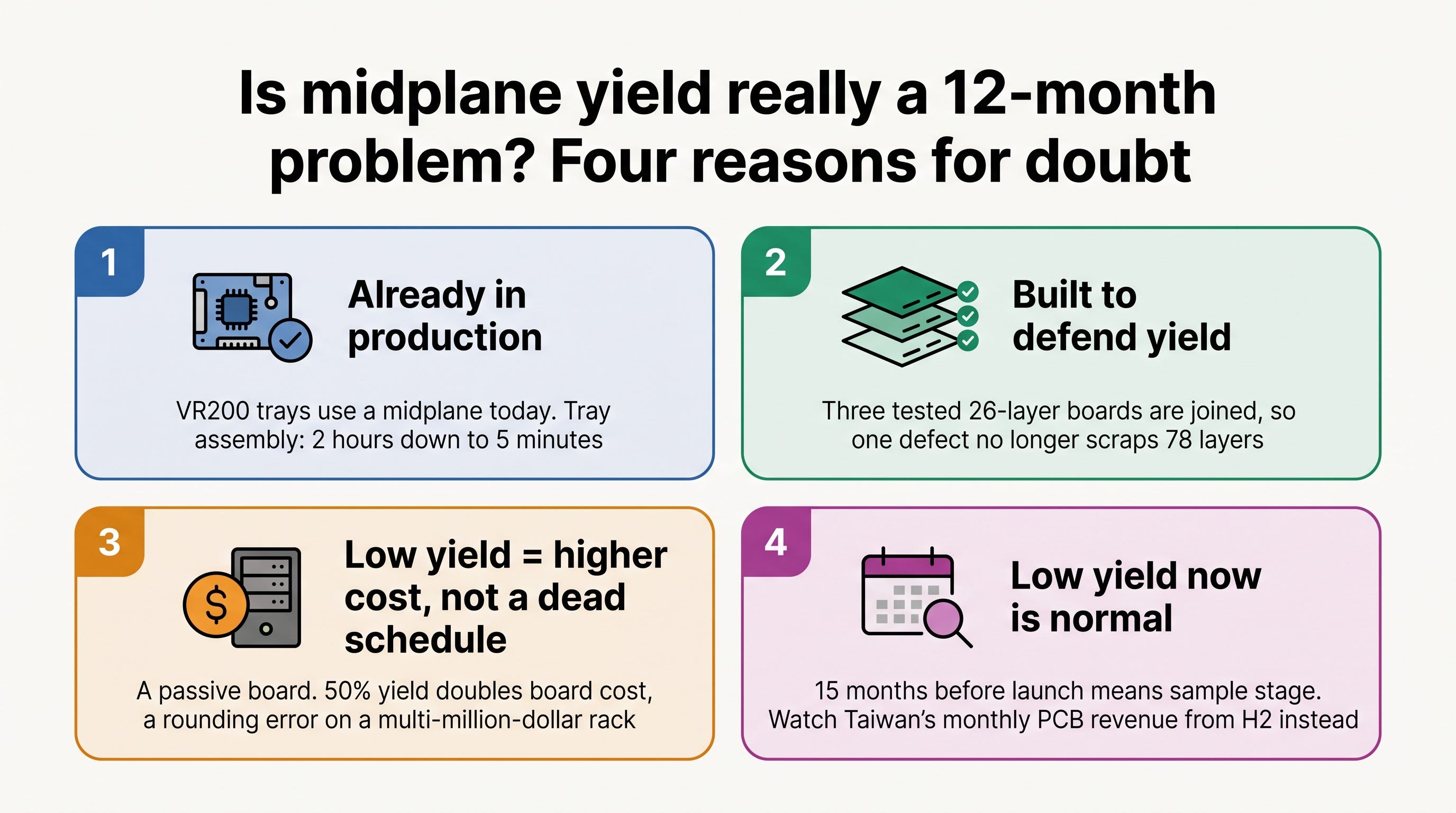
First, the midplane approach itself is already in production validation. The compute trays of the VR200 NVL72 shipping this year are already a midplane-based, cable-free design, and Jensen Huang personally highlighted at his CES 2026 keynote that this cut tray assembly time from two hours to five minutes.
The small midplane has already graduated to marketing material. What remains in question is one thing: the yield when you scale it to one square meter and 78 layers.
Second, the 78-layer spec is itself a yield-defense design. Building three 26-layer boards separately and laminating them means, under standard practice for high-layer-count boards, you can electrically test each sub-board and join only the known-good ones.
The final yield then no longer collapses as the product of all 78 layers’ process steps. It separates into the yield of the lamination and alignment steps. The chain of defect probability gets cut in the middle, by design.
Third, the economics mean low yield doesn’t kill the schedule. The midplane is a passive component with no active silicon. A 50 percent yield doubles the cost of the board, but on a rack costing millions of dollars, that is not the line item that breaks the cost structure.
The natural consequence of poor yield is higher cost and constrained early volume. For it to translate into a 12-month delay, yield would have to be bad past the point of economics and into physical unmanufacturability. With boards of the same family already running on production lines, I put low odds on that scenario.
Fourth, the timeline. A board for a product launching in the second half of 2027 should, right now, be at the engineering sample and qualification stage, where yields are always low. The observation that “it’s hard to make today” is true of every leading-edge component 15 months before launch, so on its own it is not evidence of a delay.
The diagnostic signals come next. If the schedule is real, orders and capacity expansion should start leaving traces at Taiwan’s high-layer-count PCB makers and CCL (Copper Clad Laminate) suppliers from the second half of this year. Taiwan is one of the few markets in the world where listed companies must disclose monthly revenue, around the 10th of each month, so those traces show up month by month, no need to wait for quarterly earnings.
So here is my judgment. The observation that the midplane is hard to build is probably true. But the logic that translates that observation into a 12-month delay and an opening for competitors does not hold up within SemiAnalysis’s own claims, and sentences that can be walked back no matter the outcome were sold to the market as a confirmed disaster.
The question with actual information value in this debate is which way the 2027 rack mix tilts, Kyber or Oberon. The answer will show up in Taiwan’s monthly board supply chain revenue in the second half of this year, well before any GTC keynote. I’ll be watching those numbers.
Semi Analysis is probably funded by hedge funds. My observation is that the street’s expectations were too high to start with (optical replaces copper), then when the industry tried to temper that expectation with reality of gradual shift, they seemed to move to other extreme, to suggest the lack of demand or capex. They were wrong in both instances. The companies (semi as well as hyperscalers) are chugging along at high speed, andno one is sitting around taking a breeze. Some companies valuations dont make sense true, but there also seems to be a motivated push to panic AI investors
This in-depth article is interesting and thought-provoking. I look forward to reading your writing every single morning.