

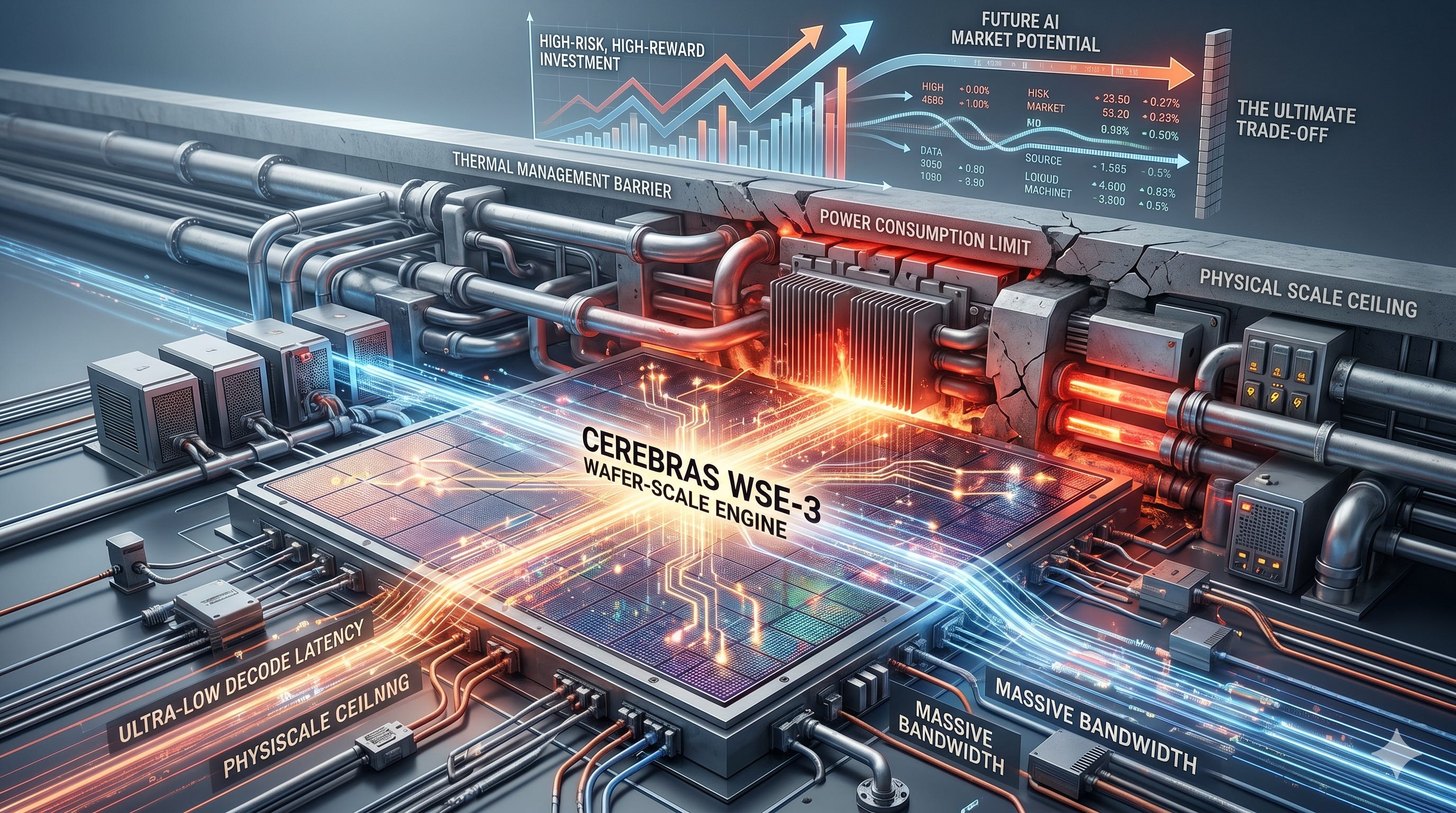
Cerebras Systems’ WSE-3 hit 2,522 tokens/s per user on Llama 4 Maverick inference. That is more than double the 1,038 tokens/s NVIDIA published for the DGX B200 on the same model.
The two benchmarks ran under different conditions (batch size, precision, whether speculative decoding was applied), so a straight comparison calls for caution. But on public benchmarks, Cerebras clearly sits at the top tier for inference decode speed.
The money followed the speed.
OpenAI signed a multi-year compute purchase agreement worth more than $20B. AWS announced it would deploy Cerebras as a decode accelerator on Amazon Bedrock. Revenue reached $510M in 2025, up 76% year over year.
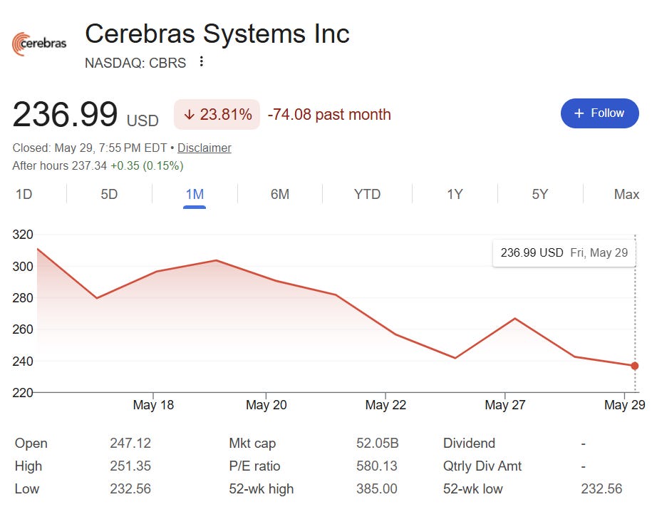
The company went public on Nasdaq on May 14, 2026.
The IPO priced at $185 and closed its first day at $311.07.
As of May 29, the stock sits at $236.99, putting market cap at roughly $52B on outstanding shares.
Cerebras is built on a fundamentally different structure from conventional semiconductors. It uses an entire wafer as a single chip, which brings a lot of technical context that has to be unpacked.
Plenty has been written about Cerebras, but most of it centered on IPO details and benchmark numbers.
There has been almost no technical analysis of what tradeoffs the defect-tolerant design actually creates, how the redundancy and repair structure affects yield and performance, or why edge defects and scribe lines become a problem at wafer scale.
I studied semiconductor DFT (Design for Test) such as defect-tolerant and repair structure design and I have worked on yield analysis, and post-silicon debug.
That work connects directly to the core issues in this architecture. This article draws on that experience to cover both what Cerebras achieved and the physical ceiling that achievement runs into.
At the end, I lay out the investment view that comes out of this technical analysis.
Disclaimer
This article is content for technical analysis, not investment advice. All investment decisions and their outcomes are the reader’s own responsibility. The figures and interpretations are based on public sources, and some technical reasoning is explicitly flagged as hypothesis-level where public data is insufficient.
1. The Problem WSE-3 Solved
The fundamental bottleneck in GPU inference: the memory wall
To generate a single next token in the decode stage of LLM inference, you have to read the model’s entire weights from memory and hand them to the compute units. Serving a 70B parameter model in FP16 (16-bit, storing each parameter in 2 bytes at standard precision) takes about 140GB just for the weights. The whole thing gets swept on every single token.
The GPU has compute capacity to spare. The bottleneck is memory bandwidth. H100 SXM’s HBM3 bandwidth is about 3.35 TB/s, H200 is 4.8 TB/s, B200 is 8 TB/s. It climbs every generation, but the structural bottleneck stays the same.
Cerebras’s solution
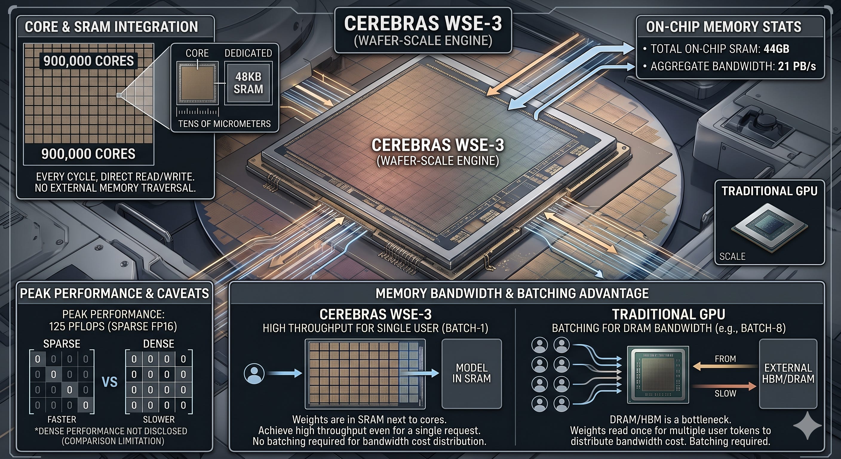
WSE-3 puts 44GB of SRAM on the chip itself. Each of its 900,000 cores has a dedicated 48KB of SRAM, with tens of micrometers between core and SRAM. Nothing routes through external memory (HBM, DRAM), so each core reads and writes data straight from the SRAM next to it on every cycle. Summing the bandwidth across all 900,000 cores gives 21 PB/s on-chip.
The peak performance Cerebras publishes is 125 PFLOPS. That figure is for sparse FP16. Sparse refers to a technique that skips the zero values inside a matrix to cut down the amount of computation, and real workloads do not always reach this level of sparsity.
Cerebras has not explicitly published dense performance (the approach that computes every value without skipping), and The Register has pointed this out. So deriving a multiple by comparing it directly against GPU dense performance may not be a fair comparison. What matters is that for work bottlenecked on memory bandwidth, such as decode, the Cerebras SRAM structure holds a fundamental advantage.
On GPUs, an inference provider bundles requests from multiple users and processes them at once. This is called batching (Batch-8 processes 8 requests together). When weights are read from memory once, multiple users’ tokens get processed at the same time, spreading the bandwidth cost. With Cerebras, the weights sit in SRAM right next to the cores, so as long as the model fits in SRAM, even a single user’s request (Batch-1) can deliver high throughput.
How a 50-year-old failed idea finally worked
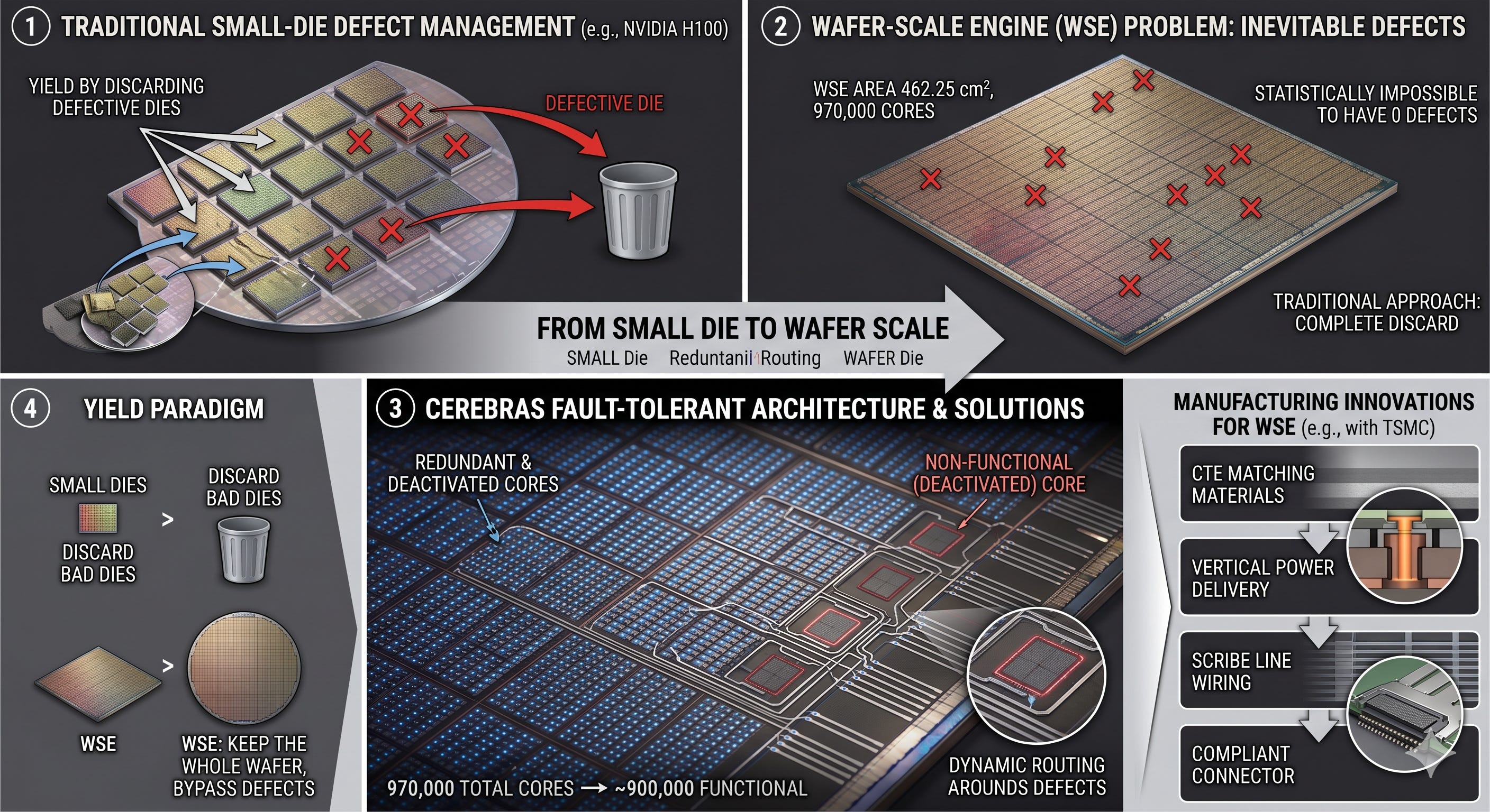
The idea of using a whole wafer as a chip failed repeatedly starting with Trilogy Systems in the 1980s. The reason is simple. Defects are unavoidable in semiconductor manufacturing. On TSMC’s 5nm process, defect density is estimated at about 0.09 per cm². Even the cleanest process produces at least this much.
NVIDIA’s H100 is about 8.15cm². Expected defects come to 0.09 × 8.15 ≈ 0.73. A fair number of dies come out with zero defects. You throw away the defective dies and ship only the good ones.
WSE-3 is 462.25cm², 57 times the H100. Expected defects come to 0.09 × 462.25 ≈ 42. The probability of zero defects is effectively zero. Every single wafer is bound to carry dozens of defects. Done the traditional way, this chip is defective the moment it is made.
WSE-3 is an architecture that started from the idea of routing around defects instead of eliminating them. The cores are made extremely small, about 0.05mm², 970,000 physical cores are laid down, and any core found defective after manufacturing is deactivated. According to Cerebras, about 900,000 cores end up operating after this process. Five manufacturing innovations made this structure possible: CTE-matched materials co-developed with TSMC over ten years, vertical power delivery, scribe-line wiring, and compliant connectors.
The structural achievements of Cerebras have been widely covered through IPO filings and company blogs.
What hasn't been analyzed is the architectural limitations this chip faces in practice.
From here, I break down the physical ceiling of the WSE-3:
SRAM capacity and quantization constraints, the bandwidth cliff when MemoryX is involved, edge defects and scribe line vulnerabilities in wafer-scale manufacturing, the qualitative shift in yield models, and the flexibility problem of fixed-hardware architectures.
At the end, I lay out the key investment variables and risks that emerge from this technical analysis.