

![Why CPO Is Becoming Inevitable? [CPO Special Part 1]](https://substackcdn.com/image/fetch/$s_!9bf7!,w_1300,h_650,c_fill,f_webp,q_auto:good,fl_progressive:steep,g_auto/https%3A%2F%2Fsubstack-post-media.s3.amazonaws.com%2Fpublic%2Fimages%2F30766732-0379-47eb-bc82-ff73fa8b10d1_900x491.jpeg)
Part 1 answered the question of why CPO exists. Now we move to the next question. If you crack open a chip package with CPO, what’s actually inside? What does each component do, and how do they all connect? And once you’ve solved the problem for switches, where does the technology go from there?
By the end of this piece, when you see terms like “optical engine,” “PIC,” “modulator,” or “external laser” in CPO news, you’ll immediately know where that component sits in the overall architecture and what job it’s doing.
Note: If you haven’t read Part 1, that’s the better place to start, especially if you’re coming from outside the field.
The Flow of Light: A Quick Map
Before diving into individual components, here’s the full picture of how light moves through a CPO system. Don’t worry if some of the terminology doesn’t land yet. Read through it once, work through the rest of the article, then come back and read this again. It’ll click.
An external laser generates pure, unmodulated light (CW light)
That light travels through a PM fiber into the PIC
Inside the PIC, the light is split and distributed across multiple channels
Each channel’s modulator encodes data onto the light, driven by electrical signals from the EIC
The modulated light travels along waveguides toward the coupling interface
It exits through the FAU into optical fiber
On the receiving end, the process runs in reverse: light arrives at the PIC’s photodetector and gets converted back into an electrical signal
The EIC’s TIA amplifies that signal
The host chip receives the data
1. Opening the CPO Package: What You’re Looking At
The best way to understand CPO is to look down at a finished package and go through the pieces one by one. Five things stand out.
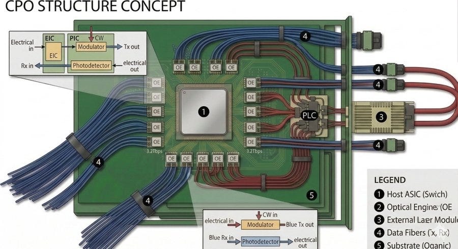
The host chip (Host ASIC) sits in the center. This is the brain of the package, the main chip everything else exists to serve. In a switch, it’s the switch ASIC. In an AI accelerator, it’s a GPU or custom AI ASIC. In a network card, it’s the NIC chip. CPO doesn’t change what the main chip is. The defining feature is simply that in a CPO package, this chip sits within a few millimeters of the optical engines.
Right now, the place in the market where CPO is most urgently needed is the scale-out network switches that connect racks to each other. Switches carry more optical ports than anything else in a datacenter, and when you have tens or hundreds of optical channels feeding into a single chip, the power and density advantages of CPO show up most dramatically. This article uses switches as the primary example, but the optical engine, laser, and PIC architecture described below is fundamentally the same whether the host chip is a GPU or a custom ASIC.
Optical engines are arranged around the host chip. These are the heart of CPO. An optical engine converts the host chip’s electrical signals into light for transmission, and on the receive side converts incoming light back into electrical signals for the host chip. Essentially, they do the job that pluggable optical modules on the front panel used to do, but from millimeters away instead of 15 to 30 centimeters. A single package can hold anywhere from eight to more than thirty optical engines, and each one typically handles several terabits per second of bandwidth.
Each optical engine contains an EIC and a PIC. The EIC is the electronic chip, handling driver circuits, TIAs, and related circuitry. The PIC is the photonic chip, handling modulators, photodetectors, and waveguides.
On the transmit side (TX): CW light from the external laser enters the PIC. The modulator inside the PIC, driven by signals from the EIC, imprints data onto the light by varying its intensity or phase. The modulator doesn’t generate light; it encodes information onto light that already exists.
On the receive side (RX): Incoming data-carrying light enters the PIC, where a photodetector converts it into electrical current. The EIC’s TIA amplifies that current into a voltage level that digital circuits can read, and that signal gets passed to the host chip.
The external laser module plugs into the front panel, outside the package. Lasers generate the light that everything else depends on, and CPO deliberately keeps them outside the optical engine for reasons covered below. Light from the laser module travels through specialty fiber into each optical engine’s PIC.
Optical fiber carries data light out of the package to the network, and brings incoming data light back in. A single optical engine connects to dozens of individual fibers, so across the whole package you’re looking at hundreds of fibers in and out.
The package substrate is the platform everything mounts on. The host chip, optical engines, power delivery circuits, and everything else sit on a single substrate, connected by fine copper traces. The critical point in CPO is that the electrical path between the host chip and the optical engines doesn’t cross a board. It stays inside the package, measured in millimeters. That short distance is what makes the power, signal quality, and port density improvements possible.
2. The Optical Engine: EIC and PIC
The optical engine is CPO’s most critical component, and it contains two distinct chips.
EIC: The Electronic Chip
The EIC handles electrical signals. It takes high-speed data from the host chip and conditions it into a form that optical components can work with.
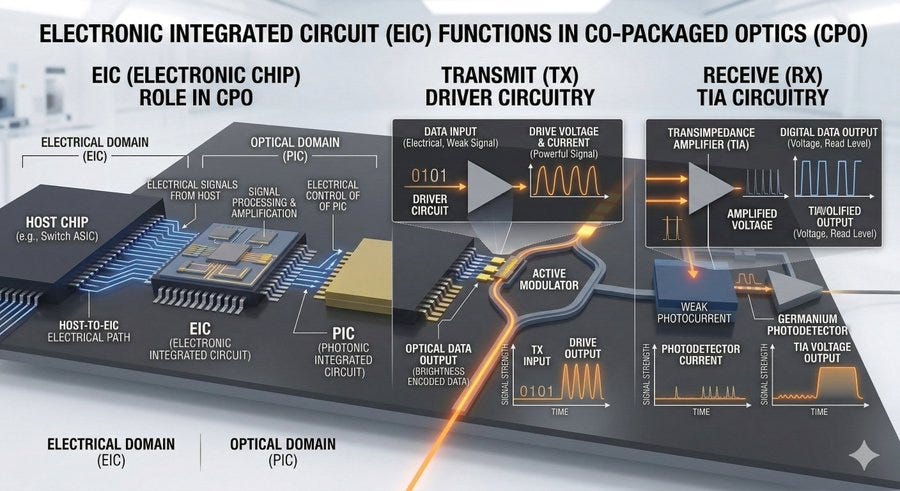
On the transmit side, driver circuits reshape the electrical signal to the right amplitude and waveform to drive the modulator. On the receive side, a TIA (Transimpedance Amplifier) takes the tiny photocurrent generated by the photodetector and amplifies it into a voltage level readable by digital logic.
EIC designers: Broadcom, NVIDIA (in-house); Alphawave Semi (for Lightmatter’s L200, SerDes IP)
One important point here. Conventional pluggable optical modules contain a heavy DSP chip. The reason is that electrical signals traveling 15 to 30 centimeters to the front panel get degraded significantly, and recovering those signals requires substantial computation. In CPO, the electrical path between the host chip and optical engine is only a few millimeters. Signals arrive essentially intact, so the DSP can be eliminated entirely or reduced to something far lighter. This is one of the core reasons CPO uses much less power: all the energy that used to go into signal recovery simply goes away.
PIC: The Photonic Chip
The PIC is where light is actually manipulated. If conventional semiconductor chips work with electrons, the PIC works with photons. Several optical components are integrated onto a single chip.
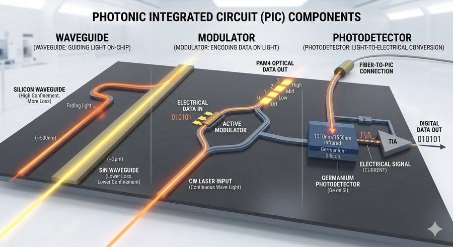
Waveguides are the roads light travels on inside the PIC. Just as optical fiber confines light within glass over long distances, waveguides on a PIC use silicon or silicon nitride (SiN) to confine light within channels a few hundred nanometers to a few micrometers wide, on the order of one-hundredth the width of a human hair. Every optical component on the PIC connects through these waveguides.
The choice of waveguide material matters. Silicon waveguides confine light tightly, which keeps them small, but they have somewhat higher propagation loss. SiN waveguides have lower loss but require more space. The choice of material is one of the first decisions in PIC design.
Modulators encode data onto light. Light arriving from the external laser is pure CW light, carrying no information. The modulator’s job is to imprint zeros and ones onto it. At its simplest, this means turning light on and off: bright for 1, dark for 0. In practice, schemes like PAM4 use four intensity levels to encode two bits per symbol. The modulator is CPO’s most consequential technical decision point, covered in its own section below.
Photodetectors convert light into electrical current. Where the modulator does electrical-to-optical conversion, the photodetector does the reverse. It absorbs incoming light and generates a proportional electrical current, which the EIC’s TIA then amplifies into a usable signal. Today’s silicon photonics PICs use germanium (Ge) photodetectors as the standard. Silicon itself doesn’t absorb infrared light at the telecom wavelengths used in communications (1310nm, 1550nm), but germanium does, and it can be grown on silicon substrates with good compatibility. Ge photodetectors are fabricated as part of the PIC process at foundries like TSMC, GlobalFoundries, and Tower Semiconductor.
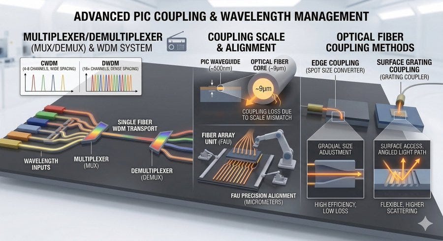
MUX/DEMUX components combine and separate light of different wavelengths. To send more data over a single fiber, you can generate light at multiple wavelengths simultaneously, load different data onto each, and send them all down the same fiber at once. This is WDM, Wavelength Division Multiplexing. Think of it like radio: FM 88.1 and FM 91.5 travel through the same air simultaneously without interfering with each other. The multiplexer (MUX) combines multiple wavelengths on the transmit side; the demultiplexer (DEMUX) separates them on the receive side.
There are two main WDM variants. CWDM (Coarse WDM) spaces wavelengths about 20nm apart, which keeps components simple and temperature-tolerant, but limits the fiber to four to eight wavelengths. DWDM (Dense WDM) packs wavelengths within a few nanometers of each other, supporting sixteen or more wavelengths per fiber, but demands much tighter temperature control and component precision.
Fiber coupling interfaces are where light exits the PIC into external fiber, or enters the PIC from external fiber. This is trickier than it sounds. A PIC waveguide is a few hundred nanometers wide. A single-mode fiber core is about 9 micrometers in diameter, roughly thirty times larger. Bridging that size mismatch without losing light is the central challenge of coupling.
Two approaches exist. Edge coupling sends light horizontally out of the chip’s side. A spot size converter at the chip’s edge gradually expands the optical mode to match the fiber. It’s reliable and low-loss, but you can only couple at the chip’s perimeter, which limits how many fibers you can connect. Surface grating coupling deflects light vertically out of the chip’s top surface. It’s more flexible spatially, since you can place coupling points anywhere on the surface, but tends to have somewhat higher loss.
FAUs (Fiber Array Units) are precision-aligned assemblies that attach multiple fibers to the PIC simultaneously. A single optical engine connects to dozens of fibers, and every one of them needs to be aligned to its coupling point on the PIC to within a micrometer. Even a small misalignment bleeds light and degrades performance. FAU alignment precision and the stability of the attachment process are among the most critical factors determining CPO manufacturing yield.
PIC designers/manufacturers: Broadcom, NVIDIA, Lightmatter, Ayar Labs, Celestial AI (acquired by Marvell), POET Technologies
PIC foundries: TSMC (COUPE), GlobalFoundries (GF Fotonix), Tower Semiconductor
3. Modulators: The Most Important Technical Fork in the Road
The choice of modulator is where CPO companies diverge most sharply from each other. Two approaches dominate today, with two more on the horizon as next-generation candidates.
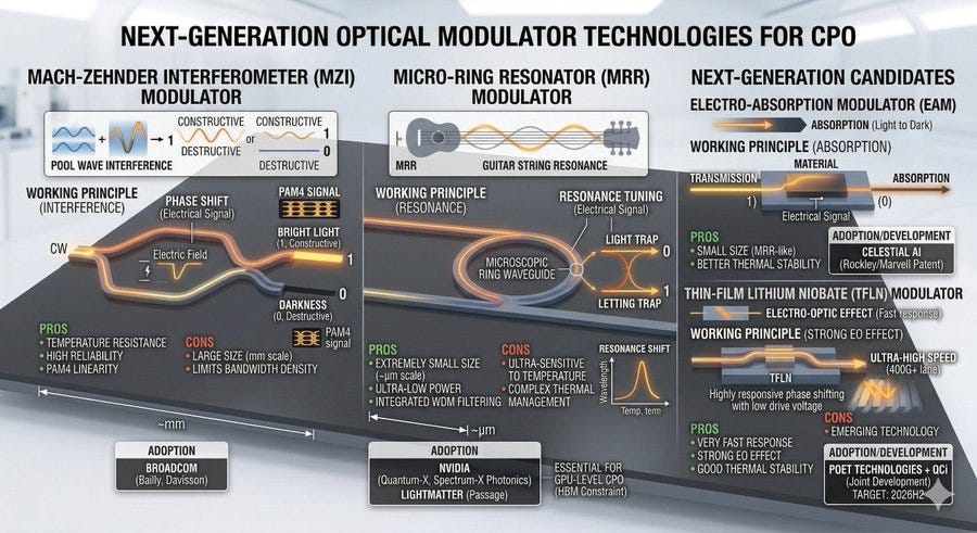
MZI (Mach-Zehnder Interferometer) Modulator
This is the most conceptually straightforward approach. Light entering the modulator gets split into two paths. An electrical signal shifts the phase of light in one path. When the two paths recombine, they either reinforce each other (producing bright light, representing 1) or cancel each other out (producing darkness, representing 0).
A useful analogy: imagine sending two waves across a pool. When the waves meet in phase, they add together into a larger wave. When they meet out of phase, they cancel each other and the water goes still. MZI modulation works the same way with light.
The strengths are thermal stability and a long track record. Temperature variation in a datacenter doesn’t meaningfully affect MZI performance. The technology has nearly four decades of validation in the telecom industry. It also handles complex modulation formats like PAM4 well, because its response is highly linear.
The weakness is size. Creating enough phase shift requires waveguide arms several millimeters long, which consumes substantial PIC area. More area per modulator means fewer channels per PIC, which limits the bandwidth density per optical engine.
MZI adopters: Broadcom (Bailly, Davisson)
MRR (Micro-Ring Resonator) Modulator
A micro-ring resonator is a tiny circular waveguide, typically five to ten micrometers in diameter. At a specific resonant wavelength, light gets trapped in the ring. An electrical signal shifts the resonance condition slightly, toggling the ring between trapping light (0) and allowing it to pass (1).
Think of a guitar string. It resonates at a specific frequency determined by its physical properties. Change those properties slightly and you shift the resonance. MRR modulators work on exactly that principle, but with light instead of sound.
The size advantage is substantial. An MRR is less than one-tenth the footprint of an MZI modulator. Far more channels fit on the same PIC area. MRRs also require lower drive voltages, which reduces power consumption, and because each ring is inherently wavelength-selective, it doubles as a filter for WDM applications, eliminating the need for a separate multiplexer.
The problem is thermal sensitivity. A one-degree temperature change shifts the resonant wavelength by roughly 0.1nm. That’s enough to detune the ring and break modulation entirely. The solution is to attach a micro-heater to each ring for real-time thermal compensation. As channel counts grow, so does the number of heaters and the power they consume, which partially offsets the MRR’s efficiency advantage. Maintaining precise thermal control of hundreds of tiny rings sitting next to a host chip dissipating several hundred watts is a genuinely hard engineering problem.
MRR-based CPO switches are now entering production. In GPU-level CPO specifically, MRR’s small footprint is nearly mandatory. GPU packages are already densely packed with HBM, leaving almost no room for optical engines. Only something as compact as an MRR can fit.
MRR adopters: NVIDIA (Quantum-X, Spectrum-X Photonics), Lightmatter (Passage)
Next-Generation Candidates: EAM and TFLN
EAM (Electro-Absorption Modulator) changes a material’s light absorption coefficient directly in response to an electrical signal, toggling between transmitting and absorbing light. It offers better thermal tolerance than MRR while still achieving reasonable density, and it avoids MZI’s size problem.
EAM development: Celestial AI (acquired by Marvell, building on Rockley Photonics IP)
TFLN (Thin-Film Lithium Niobate) Modulator replaces silicon with lithium niobate thin film as the active material. Lithium niobate has a far stronger electro-optic response than silicon, enabling fast, efficient modulation in a compact footprint with excellent thermal stability. It hasn’t reached volume production yet, but it’s the most credible candidate for 400G-per-lane and beyond, where MZI and MRR both hit their limits.
TFLN development: POET Technologies in collaboration with QCi (Quantum Computing Inc.), targeting second half of 2026
Why does the modulator choice matter this much? Because it determines PIC area, power consumption, thermal management complexity, WDM implementation approach, and ultimate bandwidth scalability, all at once. MZI’s stability suits environments where thermal management is tractable, like switches. MRR’s density suits environments where space is the binding constraint and thermals are severe, like GPU packages. The modulator choice tells you exactly what market a company is targeting and how they plan to get there.
4. The External Laser: Why Keep the Light Source Outside
Every CPO system needs a laser to generate light. In most implementations, that laser lives outside the optical engine, in a replaceable module on the front panel, rather than inside the package. This is called an ELS, External Laser Source.
Three reasons drive this design decision.
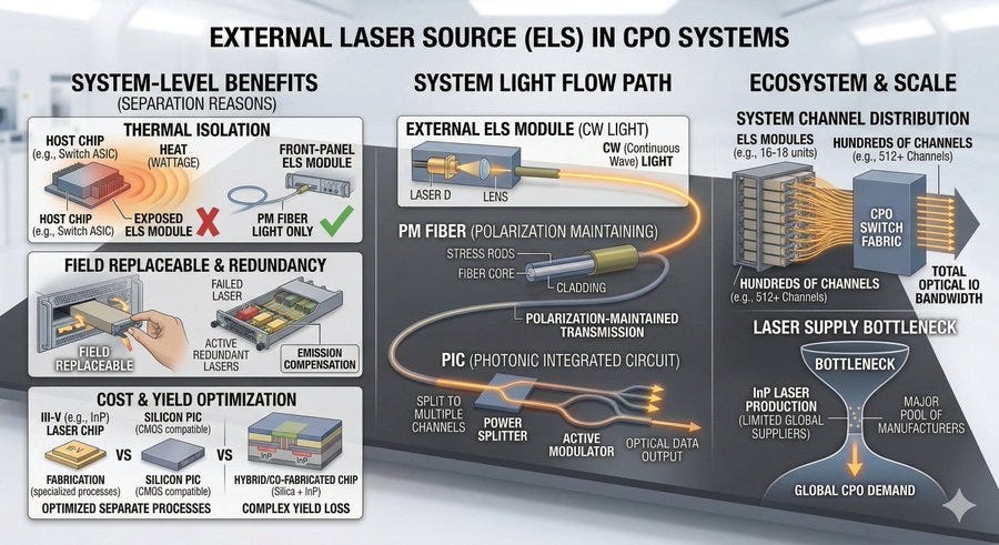
Thermal isolation. Laser diodes are extremely sensitive to temperature. Heat increases their output wavelength, reduces efficiency, and dramatically shortens lifespan. The host chip produces hundreds of watts of heat during operation. Placing a laser next to that heat source degrades it rapidly. Putting the laser on the front panel and delivering only light via fiber neatly separates the laser from the thermal environment.
Repairability. Laser diodes have shorter service lives than most semiconductor components. An external module can be replaced without touching the rest of the package. Modern CPO products make laser modules field-replaceable from the front panel, and typically include redundant laser sources within each module so that if one fails, the remaining sources compensate for the loss.
Manufacturing yield. High-quality telecom lasers are made from InP (indium phosphide) and other III-V compound semiconductors, which are entirely different materials from silicon and require different fabrication processes. Integrating lasers directly into a silicon PIC means combining two incompatible material systems, which makes the process enormously complex and kills yield. Fabricating them separately and optimizing each independently is far more practical.
Light from the external laser arrives at the PIC as CW light, pure and unmodulated. It enters through a PM (polarization-maintaining) fiber, gets distributed across multiple channels inside the PIC, and feeds into the modulators, which stamp data onto it before sending it out.
A typical CPO switch system uses around 16 to 18 laser modules, collectively supplying light to hundreds of optical channels.
Laser supply is one of the most significant bottlenecks in the CPO ecosystem. Only a small number of companies worldwide can manufacture telecom-grade InP lasers at scale, and CPO adoption will create an enormous surge in demand.
InP laser diode manufacturers: Lumentum, Coherent, Sivers Semiconductors
ELS module packaging: Lumentum, Coherent (in-house ELSFP); POET Technologies (Starlight, wafer-level packaging via Optical Interposer)
5. Packaging: Assembling All of This Into One System
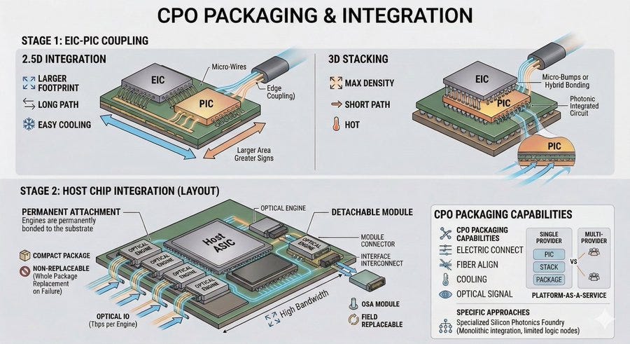
Packaging is how all the components described above, the host chip, optical engines (EIC and PIC), external laser modules, and fiber, get physically integrated into a working system. It helps to think about packaging in two stages.
Stage 1: Assembling the Optical Engine (EIC + PIC Integration)
Two approaches exist for combining the EIC and PIC.
2.5D integration places both chips side by side on a common substrate, connected by traces on that substrate. Thermal management is simpler and the fabrication process is less demanding, but the configuration takes up more area and the electrical path between the two chips is longer.
3D stacking places the EIC directly on top of (or beneath) the PIC, connected vertically through micro-bumps or hybrid bonding, a technique that joins chips at the atomic level. The footprint shrinks dramatically and the inter-chip electrical path drops to tens of micrometers. The tradeoff is that heat from both chips overlaps, making thermal management harder, and the process is significantly more complex.
The industry is moving toward 3D stacking. EICs with hundreds of millions of transistors stacked directly on top of PICs are now entering volume production.
Stage 2: Integrating Optical Engines Into the Host Chip Package
Separately from how EIC and PIC are combined inside an optical engine, there’s the question of how finished optical engines get positioned relative to the host chip.
The most common configuration places the host chip at the center of an organic substrate with optical engines arranged around it. Short substrate traces connect the host chip to each engine. Fiber exits the PIC via edge coupling at the package periphery.
Within this configuration, some designs permanently bond the optical engines to the substrate, while others use detachable module formats (OSAs, or Optical Sub-Assemblies). Permanent bonding yields a more compact package with optimized electrical paths, but if an optical engine fails, the entire package has to be replaced. Detachable modules allow field replacement, but add connectors and interface complexity that consume space. The right choice depends on what datacenter operators prioritize: density or maintainability.
Current CPO package dimensions run roughly 75mm x 75mm to 120mm x 120mm depending on the switch generation. With eight to sixteen or more optical engines per package, each handling several terabits per second, total package bandwidth reaches tens to over one hundred terabits per second.
Why Packaging Capability Is a Strategic Asset
CPO packaging requires a fundamentally different skill set than conventional semiconductor packaging. Standard packaging is purely an electrical problem. CPO packaging simultaneously demands precise fiber alignment, preservation of the PIC’s optical characteristics, and thermal management of the laser light source. The number of foundries and packaging houses that can actually deliver all of this is small, and that scarcity is exactly why packaging and foundry capability functions as a strategic moat in the CPO ecosystem.
The industry is gravitating toward integrated platforms that handle PIC fabrication, EIC-PIC 3D stacking, and full package integration under one roof. Companies building on such platforms avoid the complexity of coordinating separate foundry and packaging vendors, which compresses development timelines and cuts cost.
Integrated platform: TSMC COUPE (adopted by NVIDIA, Broadcom, Ayar Labs)
Some foundries also offer monolithic silicon photonics processes that integrate electronic and optical components on a single chip within the same fabrication run. This eliminates the need for separate EIC and PIC chips entirely, though the tradeoff is that these processes don’t support leading-edge logic nodes like 3nm or 5nm.
Monolithic platform: GlobalFoundries GF Fotonix (used for Lightmatter Passage)
Test and verification equipment: Keysight Technologies
Photonic EDA tools: Synopsys, Cadence, Ansys (Lumerical)
Conclusion
That’s everything visible when you open a CPO package. To put it plainly, CPO is not a single breakthrough component. It’s a precision integration of many technologies working in concert. The host chip’s SerDes generates high-speed electrical signals. The EIC translates those signals into a form optical components can use. The PIC’s modulator encodes data onto laser light. The photodetector converts received light back into electricity. And all of it gets assembled into a single package through micrometer-precision fiber alignment and thermal management that has to work reliably at datacenter scale. Pull out any one piece, or let any one piece fall below spec, and nothing works.
This is also why no single company can own CPO entirely. The modulator alone splits into four technical camps: MZI, MRR, EAM, and TFLN. The laser requires a completely different material system from the rest of the package. Packaging demands capabilities that span both electrical and optical engineering. Who controls which pieces of this puzzle will ultimately determine who wins in the CPO era.
Part 3 covers where this architecture goes beyond switches, and why each step of that expansion gets progressively harder to pull off.
how you fabricate these pics?using AI or self made?