

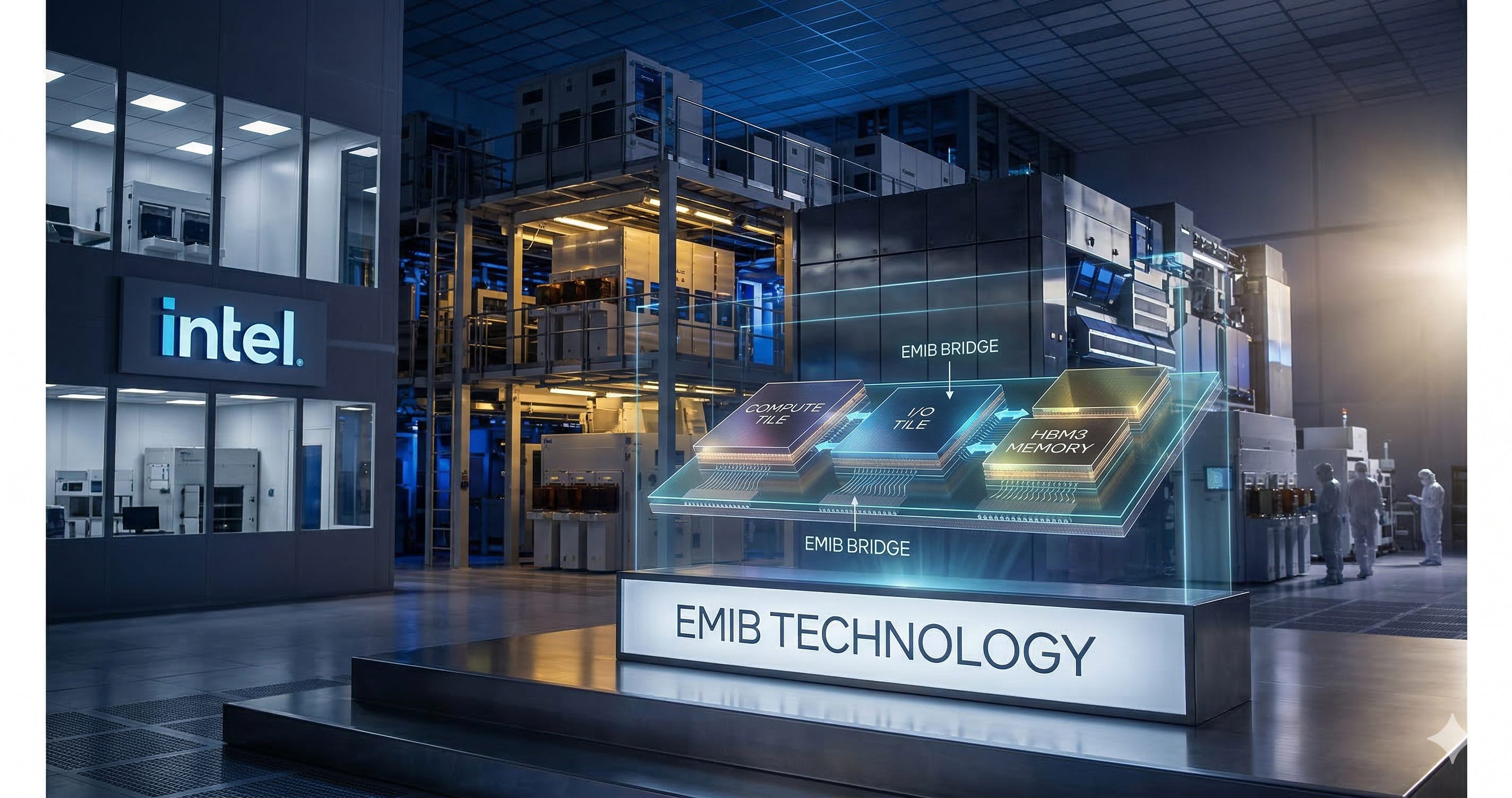
The bottleneck in the semiconductor industry has shifted. For a long time, almost everything came down to how small you could make a transistor. That’s no longer the whole story. Increasingly, what matters is how fast and efficiently you can connect multiple chips inside a single package. Packaging has become a critical competitive axis.
The dominant technology in this space is TSMC’s CoWoS (Chip on Wafer on Substrate). NVIDIA’s AI GPUs, AMD’s accelerators, Broadcom’s custom ASICs — most high-performance AI chips today are packaged using CoWoS. The problem is supply can’t keep up with demand. By industry estimates, NVIDIA absorbs a substantial portion of available CoWoS capacity, leaving other customers struggling to secure allocation. This has been going on for a while now.
Into this gap steps Intel’s EMIB (Embedded Multi-die Interconnect Bridge). In March 2026, Intel CFO David Zinsner told the Morgan Stanley conference that the packaging business was shaping up to be significantly larger than originally anticipated. Multiple outlets reported that Intel’s EMIB was being evaluated for NVIDIA’s next-generation architecture.
This piece breaks down what EMIB is, how it differs from TSMC’s approach, and what it could mean for Intel Foundry.
Substack is currently in a trial phase, so all premium quality articles are available for free for now. Once paid subscriptions are introduced, pricing will be set at a level comparable to professional tech writers on Substack. Early supporters will have the benefit of locking in their current pledge price for future paid access.
1. Why Advanced Packaging Suddenly Matters
Some context first.
AI-era chips can’t perform on their own. Take a single NVIDIA GPU: the logic die handling computation and the HBM (High Bandwidth Memory) storing data need to exchange information at extreme speeds inside one package. Advanced packaging is what makes that connection possible.
Why Advanced Packaging is the New Frontier of the AI Era

Just a few years ago, the semiconductor industry’s biggest talking point was “which company will capture the leading-edge nanometer process first.” Every semiconductor company rushed to emphasize how many nanometers their products were. However, in 2026, intertwined with the AI era, the semiconductor industry’s paradigm is passing through a clear turnin…
The old approach was monolithic design — pack everything into one large chip. But as chips get bigger, defect rates climb and costs spike. So the industry changed course. Instead of one large chip, you build multiple smaller chips (chiplets), each optimized for a specific function, and assemble them within a package. Think of it as LEGO blocks. The quality of the connections between those blocks determines total system performance.
2. CoWoS vs EMIB: Highway vs Bridge
There are several ways to connect chips inside a package. The two that matter most right now are TSMC’s CoWoS and Intel’s EMIB. To understand the difference, you need to understand interposers.
What Is an Interposer?
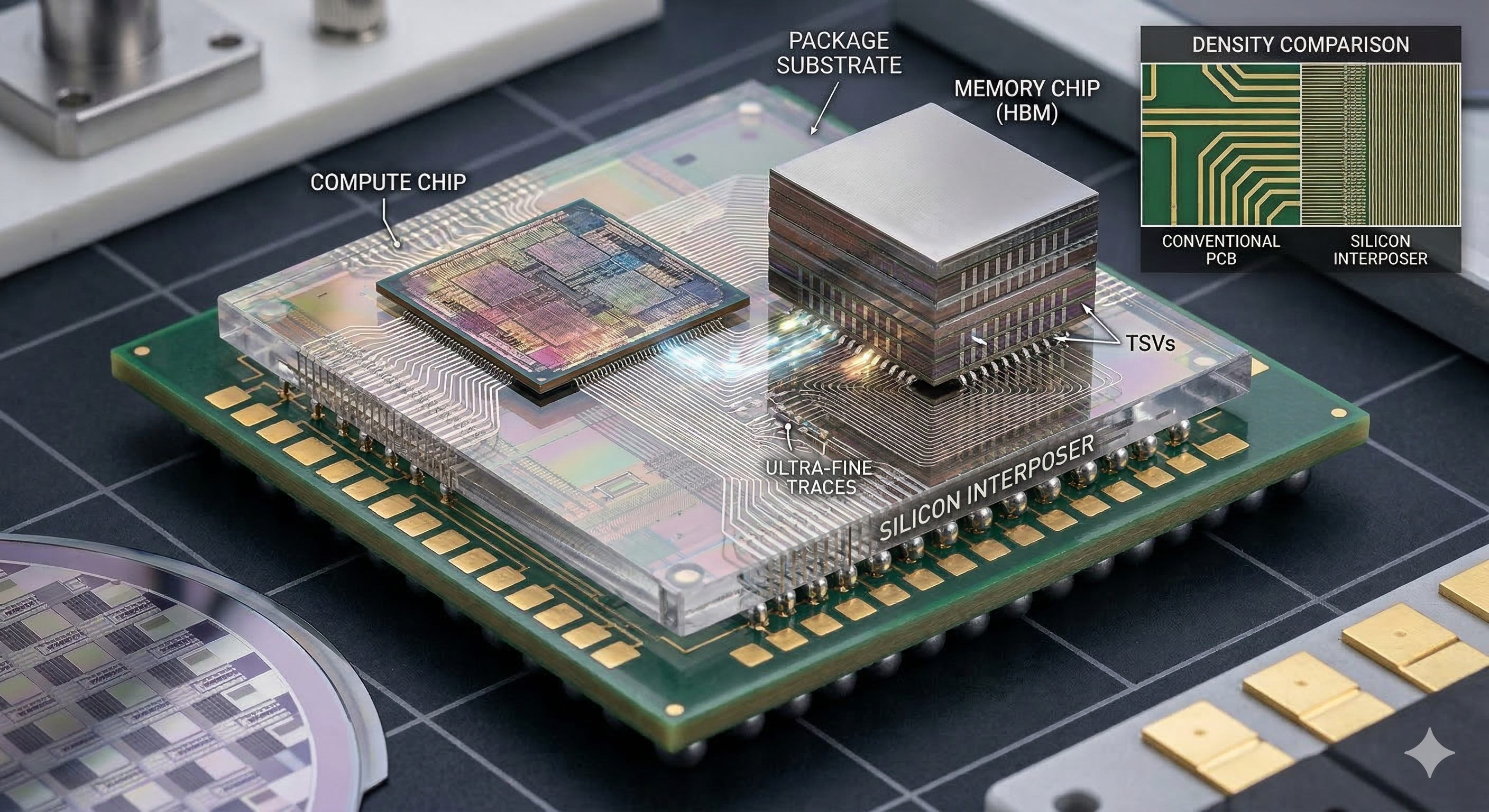
An interposer is essentially a middleman substrate placed between chips. You put a compute chip and a memory chip on top of this substrate and route data between them through extremely fine metal traces embedded in the substrate. Because the traces are much denser and shorter than what you’d find on a standard PCB, data moves faster and power consumption drops.
The question is what you make the interposer out of. Silicon enables extremely fine traces and delivers excellent performance, but silicon interposers are expensive. They’re fabricated on semiconductor wafers using processes similar to chip manufacturing itself. Larger interposers mean higher defect probability and sharply rising costs.
CoWoS: TSMC’s Approach
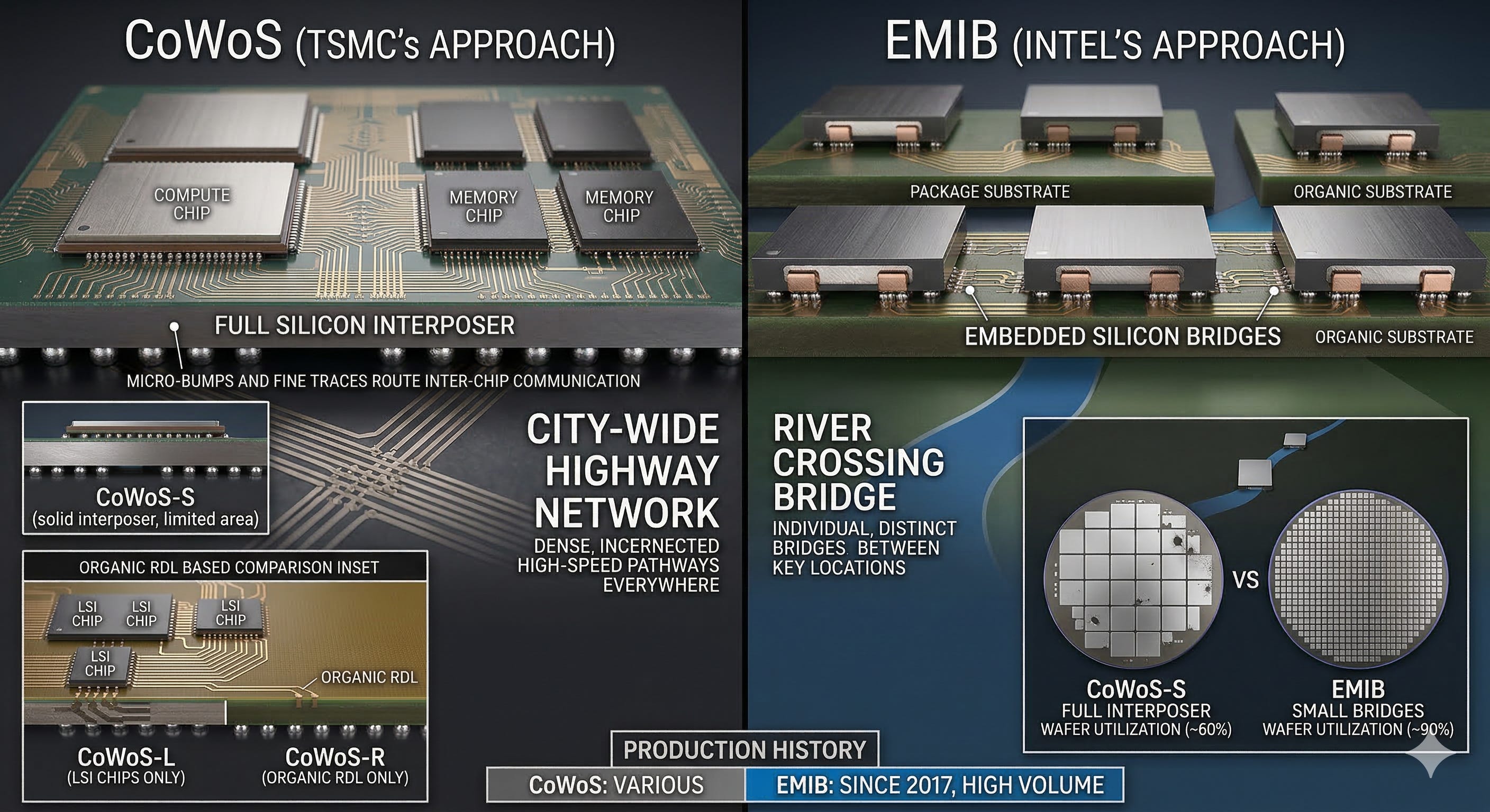
TSMC’s CoWoS places a large silicon slab beneath all the chips in the package, routing inter-chip communication through extremely fine traces embedded in that slab. Think of it as building a city-wide highway network: high-speed movement is available everywhere, but construction costs are steep.
CoWoS comes in several variants. CoWoS-S uses a solid silicon interposer and is what powers chips like the NVIDIA H100 and AMD MI300. It tops out at roughly 2,700mm² due to the reticle limit, the maximum area a lithography tool can expose in one shot. CoWoS-L extends beyond that constraint by placing small silicon chips (LSI chips) only at the high-speed interfaces and filling the rest with organic RDL. CoWoS-R goes further, replacing the silicon interposer entirely with an organic RDL layer, trading performance for cost.
Worth noting: CoWoS-L’s approach of placing silicon only where needed looks a lot like EMIB. AnandTech called it “TSMC’s answer to EMIB.” That TSMC built it at all is an implicit acknowledgment that full-area silicon interposers have limits.
EMIB: Intel’s Approach
Intel’s EMIB starts from the opposite premise. No interposer. Instead, small silicon bridges are embedded directly into the package substrate, appearing only where two chips need to talk at high speed. Everything else runs over standard organic substrate. If CoWoS is a city-wide highway network, EMIB is a bridge at a river crossing.
The practical difference shows up in utilization. Intel puts EMIB bridge wafer utilization at around 90%, versus roughly 60% for large interposers. Small pieces tile cleanly on a wafer with minimal waste, and since a significant chunk of CoWoS packaging cost comes from the silicon interposer, eliminating it changes the cost structure.
EMIB has been in production since 2017, starting with the Stratix 10 FPGA and running through server CPUs including Sapphire Rapids and Granite Rapids. Years of high-volume production history matter when an external customer is deciding whether to trust a packaging partner with their flagship chip.
What’s Actually Different
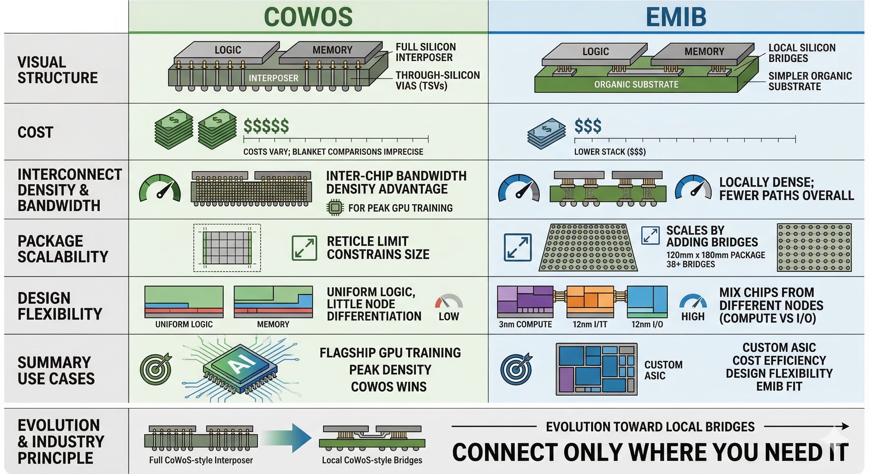
Cost: CoWoS carries higher packaging costs due to the large-area silicon interposer. EMIB is structurally cheaper because that interposer doesn’t exist. Actual cost differences vary by design and configuration, so blanket comparisons are imprecise.
Interconnect density: CoWoS allows traces across the entire interposer area, giving it an advantage in inter-chip bandwidth density. For GPUs requiring extreme throughput, CoWoS remains the better option.
Package scalability: EMIB scales by adding bridges wherever they’re needed. Intel’s EMIB-T specification supports a 120mm x 180mm package with 38 or more bridges. CoWoS-S is constrained by the reticle limit on interposer size, and while CoWoS-L extends that, it hasn’t matched EMIB’s scalability.
Design flexibility: EMIB allows mixing chips from entirely different process nodes in one package. A compute die on 3nm and an I/O die on 12nm can coexist. Each bridge connection can be individually optimized. For custom ASIC design, this flexibility has real value.
CoWoS and EMIB are not substitutes for each other. They address different use cases. For flagship GPU training chips demanding peak interconnect density, CoWoS wins. For custom ASICs where cost efficiency and design flexibility matter more, EMIB is the better fit. What’s interesting is that CoWoS is evolving toward EMIB’s core idea (local silicon bridges rather than full-area interposers). The principle of “connect only where you need it” is being absorbed by the broader industry.
3. How EMIB Is Evolving
EMIB is not static. As AI chip requirements change rapidly, the technology has branched in several directions.
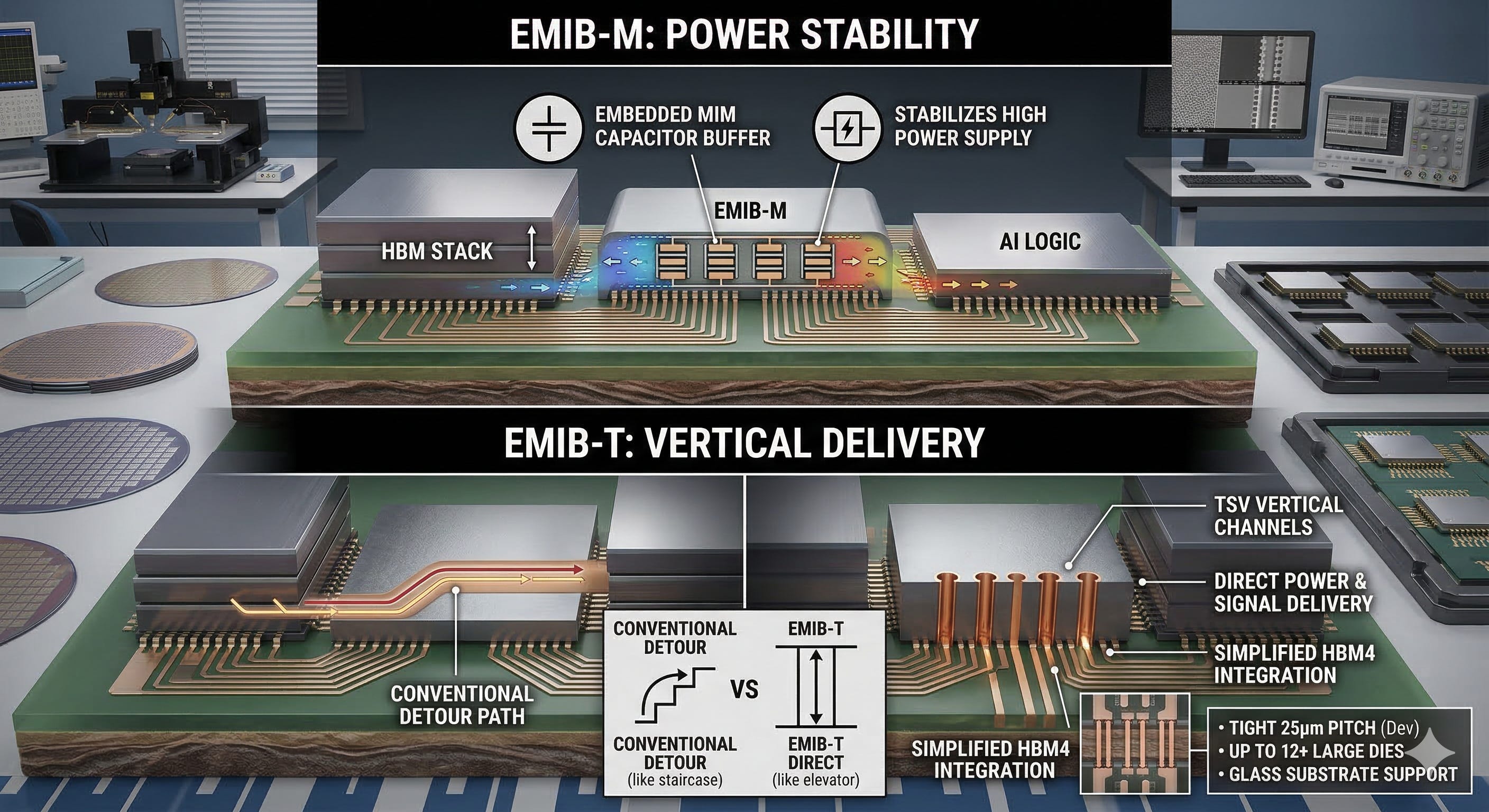
Better Power Stability: EMIB-M
AI chips consume enormous power, and the problem isn’t consumption per se but the instability that comes with it. Noise on the power delivery network directly affects chip performance and reliability.
EMIB-M addresses this by embedding MIM capacitors (Metal-Insulator-Metal Capacitors) inside the bridge itself. Capacitors store charge temporarily and release it on demand. Integrating them into the interconnect acts as a power buffer, stabilizing supply to the chips. Think of it as embedding a voltage regulator directly into the connection layer.
Vertical Power Delivery: EMIB-T
The more significant evolution is EMIB-T, where “T” stands for TSV (Through-Silicon Via).
In conventional EMIB, signals and power travel laterally along the bridge surface, taking a detour to reach their destination. It’s like going from a building’s basement to its roof by walking up an external staircase. EMIB-T drills vertical through-holes (TSVs) through the bridge itself, allowing signals to travel straight through. The elevator shaft, rather than the fire escape.
Two things improve substantially. First, the power delivery path shortens and resistance drops. In the original EMIB “cantilever” geometry, power had to travel around the bridge to reach the chip. In EMIB-T, power comes from below through TSVs directly. For high-wattage AI chips, this is a meaningful difference. Second, integration with next-generation HBM4 and HBM4e becomes more natural. HBM itself stacks multiple DRAM layers using TSVs, so having TSVs in the connecting bridge simplifies the interface geometry.
EMIB-T’s specs are notable. Packages up to 120mm x 180mm with 38+ bridges and 12+ large dies. Bump pitch has tightened from 55μm in the first generation to 45μm and now 35μm, with 25μm in development. It also supports glass substrates in addition to organic ones, which matters because glass offers better thermal stability and enables finer routing, making it one of the key materials directions for next-generation packaging.
Combining Vertical and Horizontal: 3.5D
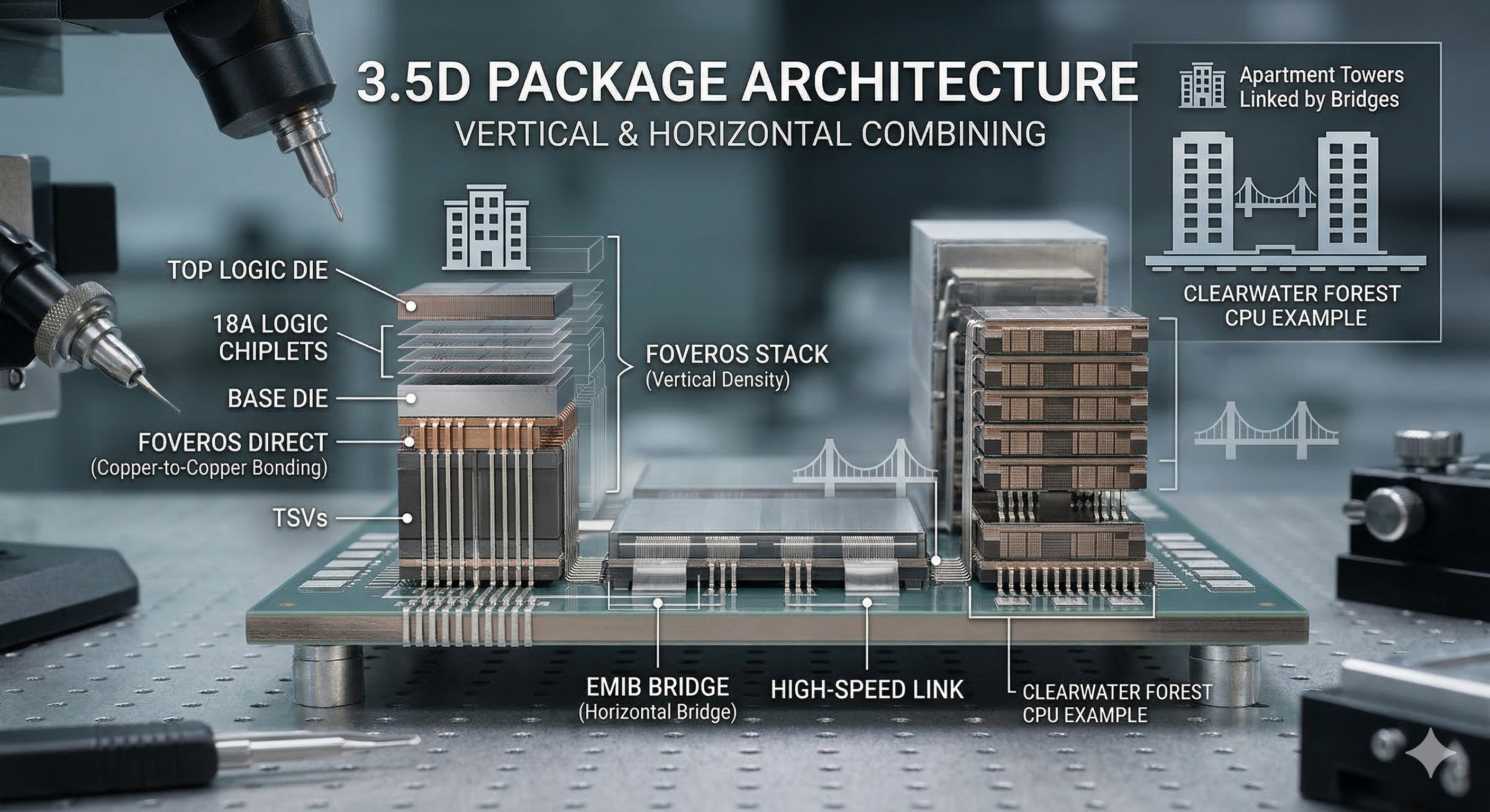
This is where Intel’s Foveros technology enters the picture.
If EMIB connects chips horizontally (the 2.5D model), Foveros stacks chips vertically (3D). Die on top of die, connected by TSVs and microbumps. The latest version, Foveros Direct, enables copper-to-copper direct bonding without bumps at all, which is what the industry calls hybrid bonding. Foveros is an Intel-developed technology that entered production in 2019 with the Lakefield processor and was later used in Meteor Lake.
Combine the two and you get 3.5D: chiplet stacks assembled via Foveros, then interconnected horizontally via EMIB. Apartment towers linked by bridges. This configuration allows vertical density increases while preserving horizontal scalability. Intel’s latest server CPU, Clearwater Forest, uses this 3.5D architecture: 18A process logic chiplets stacked on a base die via Foveros, with EMIB connecting those modules horizontally.
A Naming Collision Worth Noting
Broadcom also calls its XDSiP platform “3.5D,” which creates confusion. The underlying technology is completely different. Broadcom’s 3.5D is built on TSMC’s stack: CoWoS-L (LSI bridge + RDL interposer) for horizontal connectivity, and TSMC’s SoIC (System on Integrated Chips) for vertical stacking. SoIC is TSMC’s wafer-level direct bonding technology for 3D integration, the equivalent of Foveros in the TSMC ecosystem.
To summarize:
Intel’s 3.5D = EMIB (horizontal) + Foveros (vertical). Both are Intel technologies.
Broadcom’s 3.5D = CoWoS-L (horizontal) + SoIC (vertical). Both are TSMC technologies.
Same label, entirely different technology stacks. Always check whose technology sits underneath when you see “3.5D.”
4. EMIB and Optical Interconnects
The way chips communicate across data centers is changing. Traditional electrical signaling over copper traces is hitting walls on both bandwidth and energy efficiency. CPO (Co-Packaged Optics) is emerging as a response: optical engines placed directly inside a chip package, transmitting data via light instead of copper.