

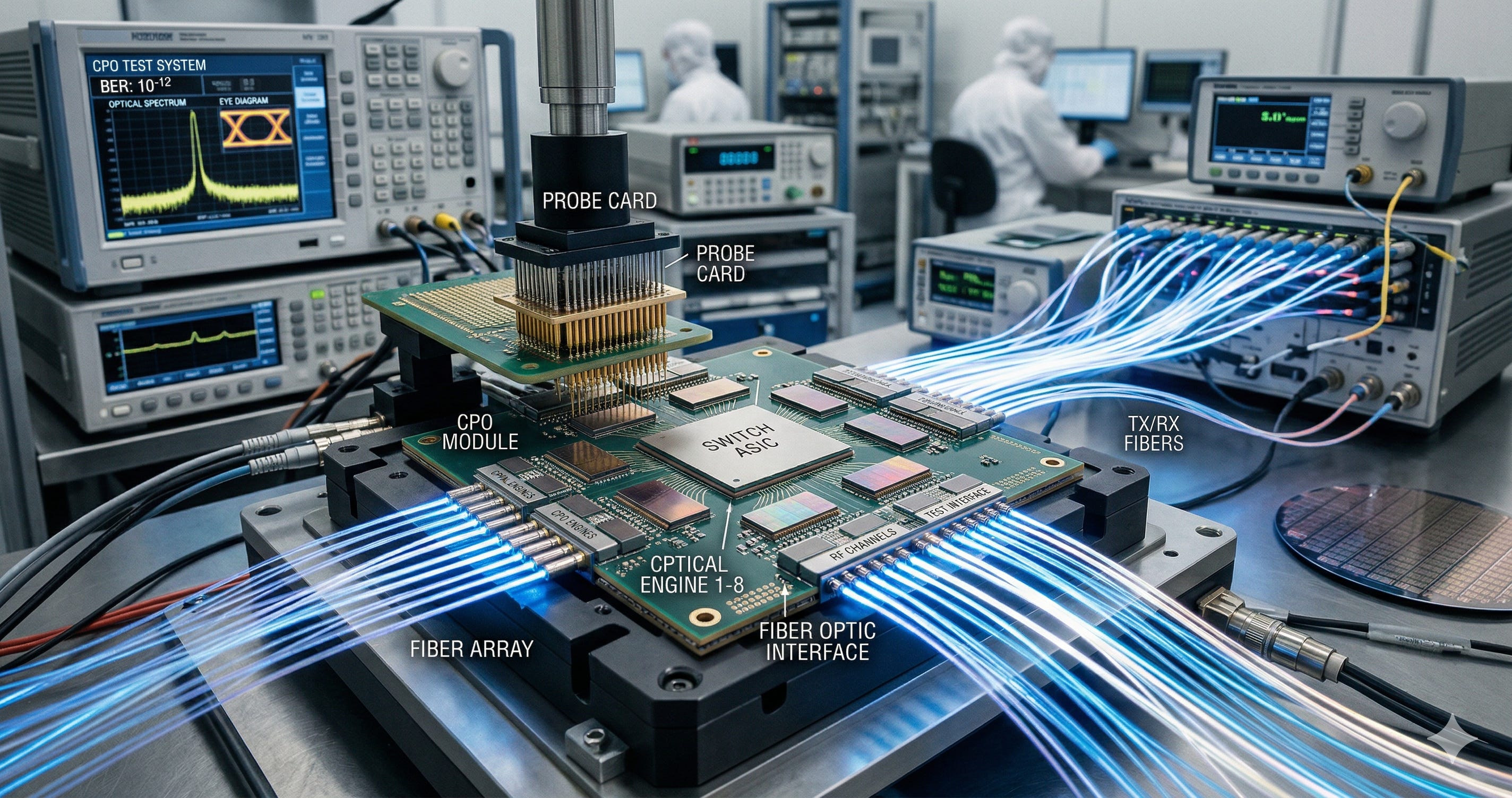
Interest in CPO (Co-Packaged Optics) is exploding.
Broadcom is in volume production with its second-generation CPO based on Tomahawk 5, and NVIDIA announced at GTC 2026 that the Quantum-X photonic switch has entered full production.
TSMC is moving its COUPE platform into volume production this year, and Samsung Foundry has announced a CPO turnkey target for 2029.
As bandwidth bottlenecks in AI data centers collide with the physical limits of copper interconnects, CPO is no longer a technology of the future. It's a production reality, integrating optics directly into ASIC packages.
But there’s one area most investors and engineers overlook: CPO testing.
Building CPO is hard enough. Testing it is a different problem entirely. Conventional ASICs are tested with electrical signals alone. CPO requires measuring electrical and optical signals simultaneously, at sub-micron precision. That’s precisely why the semiconductor test infrastructure that took 50 years to optimize is getting rewritten from scratch.

If you’ve been evaluating CPO investments by looking only at lasers, optical engines, and packaging, there’s a good chance you’ve been missing the most undervalued segment in the value chain.
This article covers why CPO testing represents an opportunity going forward, walks through the full CPO test process stage by stage, and examines which companies deserve attention at each step. If your knowledge of CPO testing has been fragmented, this article will connect the full picture.
Disclaimer
This article is a technical analysis based on publicly available information and general industry knowledge. It contains no NDA-protected or confidential information related to the author’s current employer. Nothing here constitutes a buy or sell recommendation. All investment decisions are the reader’s own responsibility.
How Conventional ASIC Testing Works
Here’s the semiconductor test flow. Once a chip is finished, it goes through three major stages.
How Do We Actually Test Semiconductors?

Have you ever wondered how semiconductor testing actually works?
First, Wafer Sort. In wafer state, probe card needles contact each die’s pads. Electrical signals go in, electrical signals come out. From open/short tests to functional tests, the ATE (Automatic Test Equipment) handles everything. Defective dies get marked with ink or flagged in a map.
Second, Package Test. After dicing and packaging, the chip goes back on the ATE. Handlers pick chips and load them into sockets, and the tester verifies all functions via electrical signals. Temperature conditions are applied too: high temp, low temp, ambient. Speed binning happens here as well.
Third, System Level Test (SLT). The chip runs in conditions that approximate a real system environment. Does it boot? Can it process actual workloads?
All three stages share one thing: they’re entirely electrical.
Probes contact pads, signals go in, signals come out. It’s the paradigm that has been optimized for over 50 years, and every ATE platform, probe card, handler, and socket in the industry was built on this assumption.
But as copper interconnects hit their limits in AI data centers, optical interconnects that transmit data using light have entered the picture. Optical signals are now intruding on test infrastructure that was designed to handle only electrical ones. To understand what this shift means, you first need to understand what an optical module actually is.
Optical Modules: PIC and EIC
Transmitting data between chips in a data center using light instead of copper requires opto-electronic conversion. That function is handled by optical modules. Inside an optical module sits an optical engine, or an equivalent opto-electronic conversion block. This article focuses on silicon photonics (SiPh)-based optical engines. A SiPh-based optical engine typically consists of a PIC (Photonic IC) and the EIC (Electronic IC) that drives it.
CPO, Fully Dissected [CPO Special Part 2]
![CPO, Fully Dissected [CPO Special Part 2]](https://substackcdn.com/image/fetch/$s_!LFif!,w_1300,h_650,c_fill,f_webp,q_auto:good,fl_progressive:steep,g_auto/https%3A%2F%2Fsubstack-post-media.s3.amazonaws.com%2Fpublic%2Fimages%2Fd2df124c-d6b0-4142-833c-908be262ab7c_900x491.jpeg)
Part 1 answered the question of why CPO exists. Now we move to the next question. If you crack open a chip package with CPO, what’s actually inside? What does each component do, and how do they all connect? And once you’ve solved the problem for switches, where does the technology go from there?
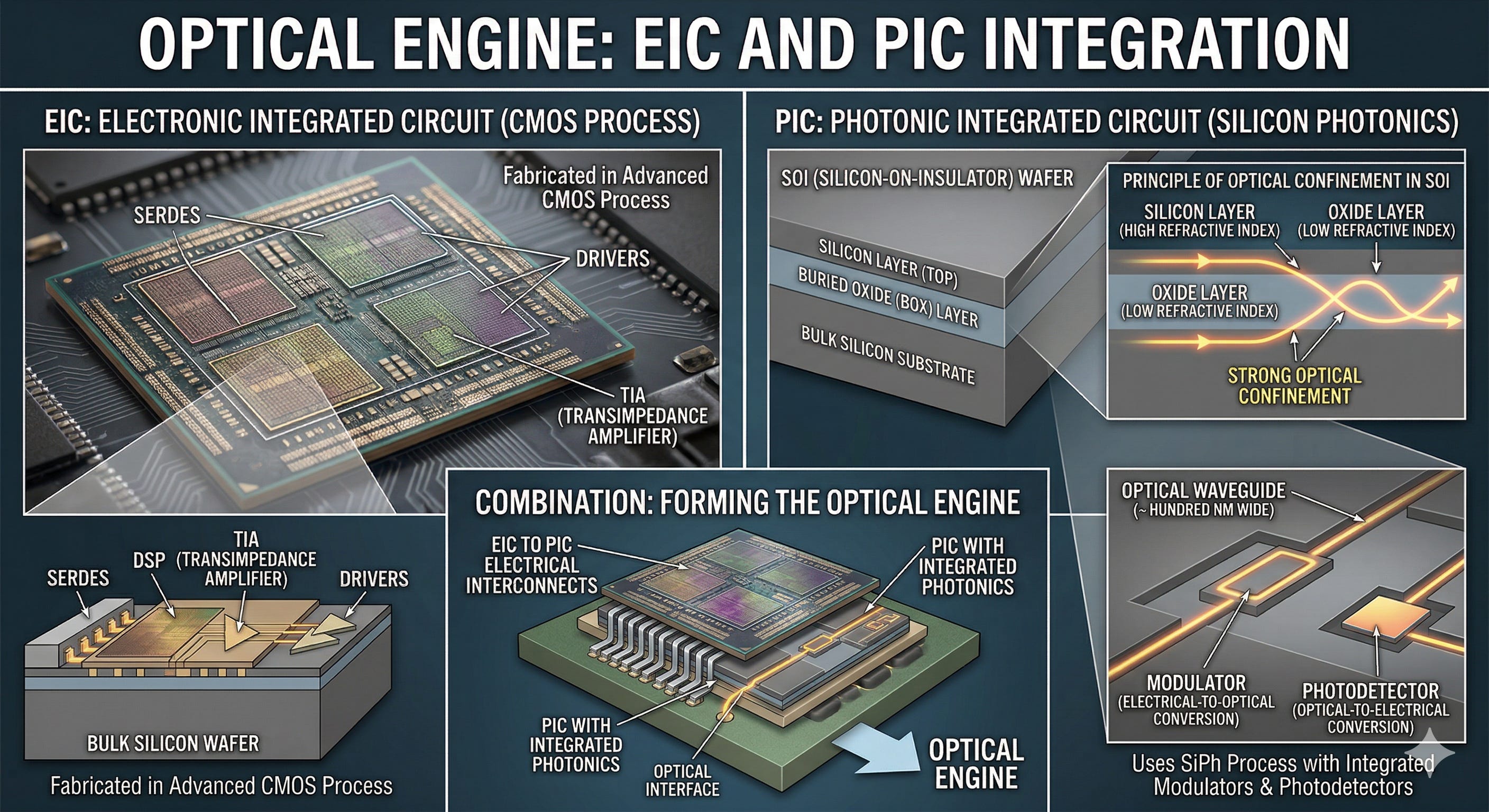
The EIC is close to what we think of as conventional semiconductor logic. It contains circuit blocks like SerDes, DSP, TIA (Transimpedance Amplifier, a circuit that amplifies the weak current from a photodetector), and drivers, fabricated in an advanced CMOS process.
The PIC is different. PICs are made using Silicon Photonics (SiPh) processes. Conventional semiconductors use bulk silicon wafers, but SiPh uses SOI (Silicon-on-Insulator) wafers. An SOI wafer has a layer of oxide (BOX, Buried Oxide) beneath the silicon layer.
The BOX layer’s refractive index is far lower than silicon’s, and this low-index layer creates strong optical confinement within the silicon layer. Using this principle, optical waveguides just a few hundred nanometers wide can be etched into the silicon layer, with modulators (devices that convert electrical signals into optical signals) and photodetectors (devices that convert optical signals back into electrical signals) integrated on top. The finished result is a PIC.
One note: silicon itself is not a favorable material for laser emission, so real-world optical engines require a separate laser source, either an external laser source module or a III-V compound semiconductor for light generation. This article covers the PIC/EIC-centered test flow; laser source testing is a separate topic and is not addressed here. For more details on lasers, please refer to the article below
The War of Light, A Laser Shortage

On March 2, 2026, NVIDIA invested $2B in Coherent and another $2B in Lumentum. Both companies make lasers. The two announcements came on the same day and included “multi-billion dollar purchase commitments” and “future capacity access rights.” Jensen Huang wasn’t just buying lasers. He was locking up the ability to make them.
The combination of EIC and PIC is the optical engine. Pluggable, NPO, and CPO all require opto-electronic conversion. The difference lies in how closely that conversion block is placed relative to the ASIC.
How the Optical Module Attaches: Pluggable, NPO, CPO
There are three configurations based on how closely the optical engine is integrated with the ASIC.
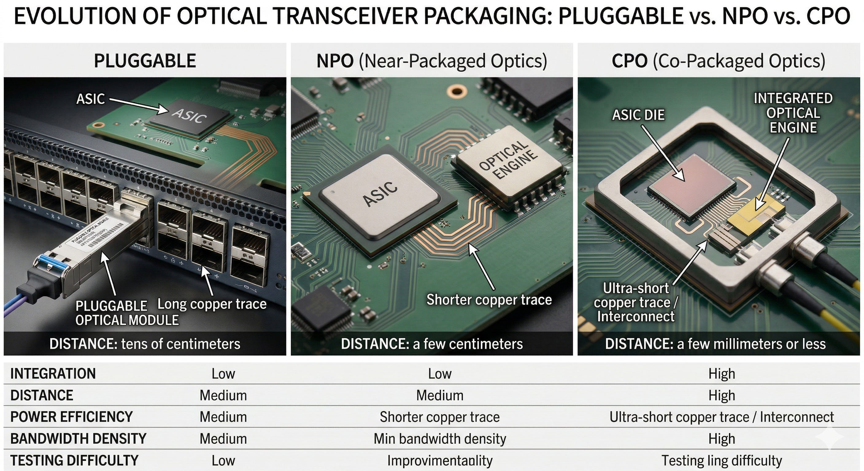
Pluggable means optical transceiver modules plug into cages on the front panel of a switch. The ASIC and module sit roughly tens of centimeters apart.
NPO (Near-Packaged Optics) is a middle-ground architecture that places the optical engine immediately adjacent to the ASIC, closing the gap to roughly a few centimeters.
CPO (Co-Packaged Optics) integrates the optical engine or optical subassembly into the same package as the ASIC, with separation on the order of a few millimeters or less. The closer the integration, the shorter the copper traces, which improves power efficiency and bandwidth density. But testing gets dramatically harder.
Here’s how each looks from a test perspective.
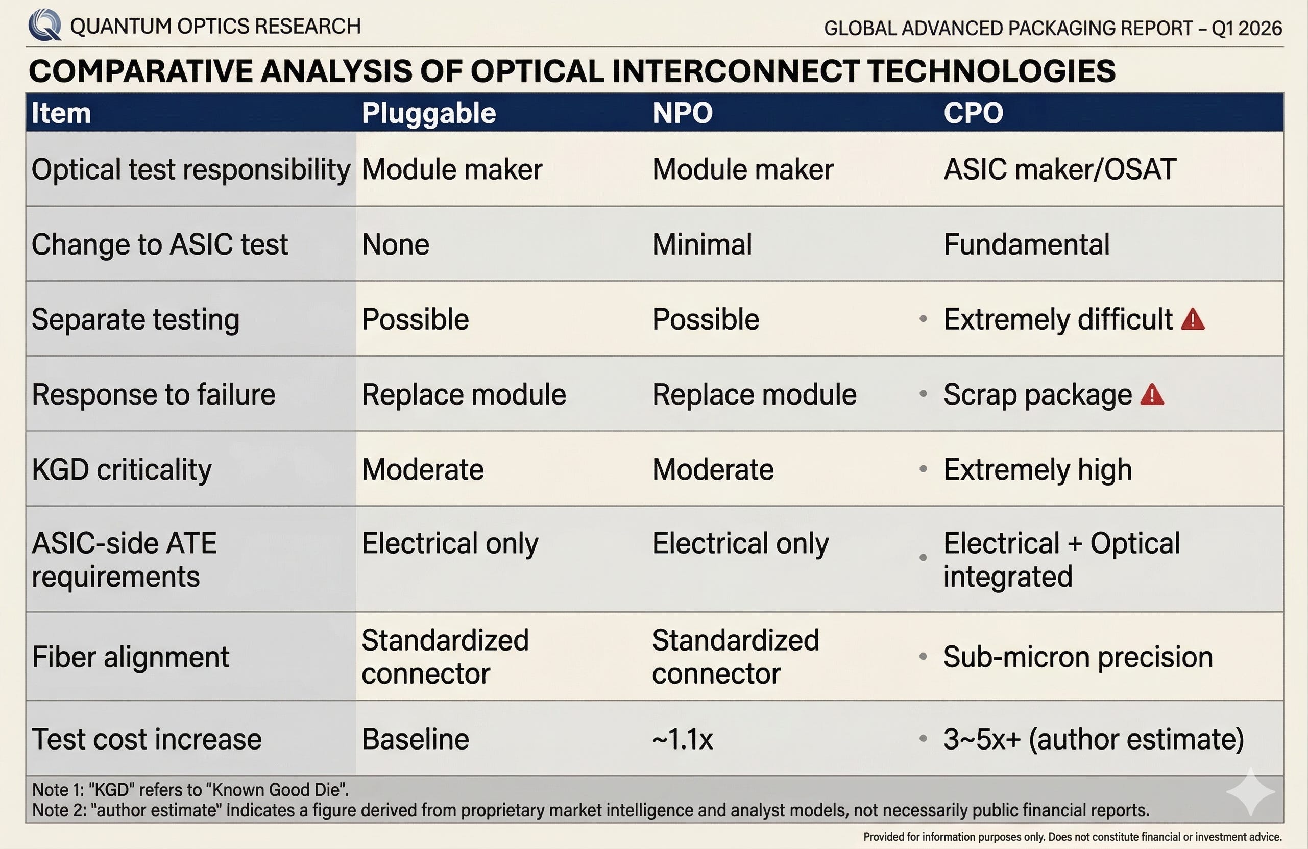
Pluggable modules are the most familiar form. Standardized transceiver modules like QSFP-DD or OSFP plug into the front panel of a switch. The ASIC and optical engine are physically separate. The biggest testing advantage is that each can be tested independently. The ASIC follows the conventional ATE flow on its own. The optical module is tested by the module maker independently. You secure a KGD (Known Good Die) and a Known Good Module separately, then assemble. If something fails, you pull the module and replace it.
NPO (Near-Packaged Optics) is a middle-ground architecture that places the optical engine directly adjacent to the ASIC. Implementations vary by vendor: some mount components on the same board in close proximity, others integrate them on a shared substrate near the ASIC package. Shorter copper traces improve signal integrity. Compared to CPO, the ASIC and optical engine are still physically separate, so independent testing and replacement remain possible. That said, differences in proximity, fiber routing, and thermal conditions mean system integration testing isn’t identical to pluggable.
CPO is a different dimension entirely. The optical engine or optical subassembly is integrated with the ASIC in the same package or first-level substrate. In NVIDIA’s Quantum-X, TSMC COUPE-based optical subassemblies are co-integrated with the switch ASIC in a single package. Total throughput: 115.2 Tbps, 144 ports at 800G.
With CPO, pulling a module and swapping it the way you would with pluggable is extremely difficult once the assembly is complete. If there’s a defect in the PIC, rework is enormously burdensome, and in practice you’re often looking at scrapping the entire high-value package.
Why CPO Testing Is So Hard
In CPO, securing a Known Good Die for the PIC before co-packaging is what makes or breaks volume production. The catch: fully verifying a PIC’s optical characteristics at the wafer level is hard. Some defects only reveal themselves after packaging. And the verification process itself is fundamentally different from conventional semiconductor testing.
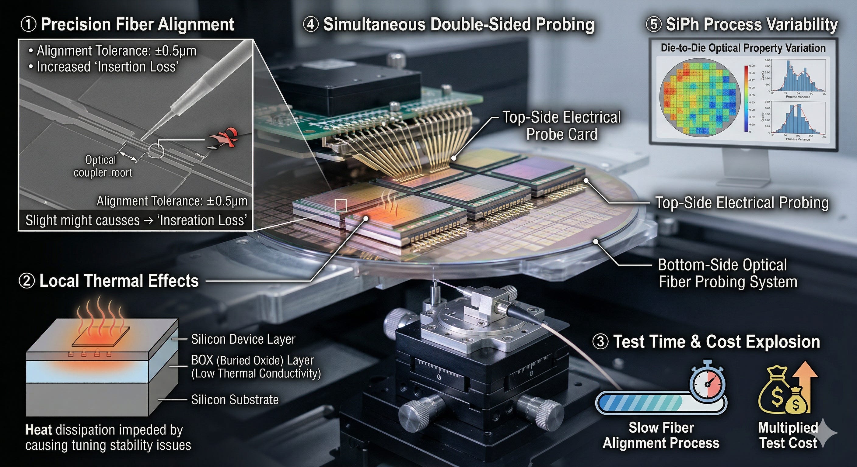
Fiber alignment. To test a PIC, you need to bring an optical fiber precisely to the coupler on the chip, the port that routes light in and out of the die. This is a completely different scale from the tens-of-microns precision of conventional electrical probe cards. Alignment tolerance varies from sub-micron to a few microns depending on the coupler structure, and even small misalignments can cause a significant jump in insertion loss. The accuracy of optical measurements is directly tied to alignment quality.
Thermal effects. Laser source wavelength is temperature-sensitive. The ring modulators inside a PIC shift their resonance wavelength with temperature changes. The SOI wafer’s BOX layer has roughly 100 times lower thermal conductivity than silicon, which impedes heat dissipation and can cause local thermal non-uniformity and tuning stability problems. In conventional ASIC testing, applying temperature conditions was about verifying device operating specs. In CPO, temperature control becomes far more critical and thermal stability is much harder to manage. The BOX layer’s low thermal conductivity can actually benefit thermal tuning efficiency in some respects, but in a test environment it makes maintaining uniform temperature significantly more difficult.
Test cost explosion. Aligning a fiber to a coupler takes time. Even with automated equipment, it’s incomparably slower than electrical probing. Add simultaneous electrical testing on top, and the fully loaded per-chip test cost, including equipment depreciation, test time, and consumables, multiplies several times over.
Double-sided probing. For wafers where EIC and PIC have been stacked via hybrid bonding, you need to probe electrical pads from the top while presenting optical fiber to the coupler from the bottom. Accessing both sides of the wafer simultaneously is something conventional prober infrastructure was never built to handle.
SiPh variability. Because SiPh process variability is high, PIC wafers show large die-to-die and wafer-to-wafer variation in optical characteristics. There is still no industry standard for test guardband optimization.
Simultaneous electrical and optical measurement, sub-micron precision, double-sided probing, active thermal management, high process variability. Conventional ATE infrastructure can’t handle it. So what stages does CPO testing actually go through, what equipment is needed at each stage, and among the companies building that equipment, who is best positioned?