

Interview 20 October 2026 · US Pacific Time · approximately 86 minutes
Interview and editing Damnang · Damnang Research
Expert Former ASML EUV light source research engineer
ASML supplies EUV systems used in advanced semiconductor manufacturing. Its strong technological position alone does not explain how quickly equipment output or profits can grow. Customers must be able to lower the total cost of their processes by adopting expensive equipment, while ASML needs to expand production capacity together with its critical component suppliers.
In this interview, we spoke for approximately 86 minutes with a former ASML EUV light source research engineer. We began with the differences between DUV and EUV and the reasons for High NA, then discussed the steps involved in installing a system at a customer fab and the service business. We also covered ASML’s pricing power, China’s economic incentives to develop its own EUV systems, and Terafab’s prospects for securing equipment and reaching mass production.
The assessment of Terafab was particularly interesting. The expert was optimistic about building a fab with the support of established equipment suppliers, but more cautious about developing equipment internally and achieving mass production in roughly two years. The assessment changes when equipment procurement, process integration and the production schedule are considered separately.
Disclaimer
The answers reflect the expert’s experience and personal views, not ASML’s official position. Additional information from public sources is identified in editor’s notes.
This report was prepared with AI assistance to summarize and organize the expert call transcript.
Contents
Experience in EUV Light Source Research and Product Development
How Chipmakers Choose Between DUV and EUV
What High NA Improves and What It Requires
From Building an EUV System to Installing It at the Customer Fab
Equipment Planning for New Fabs and Maintenance of Existing Systems
ASML’s Technological Advantage and the Conditions for Profit Growth
Why China Wants to Develop Its Own EUV Systems
Assessing China’s EUV Progress and Its Impact on Supply
Terafab’s Equipment Procurement and Prospects for Mass Production
Damnang’s Assessment
1. Experience in EUV Light Source Research and Product Development
Damnang
What did you research at ASML, and how did that technology make its way into actual systems?
Expert
I worked on EUV light sources at ASML. I joined at a time when the source architecture was changing and the results of basic research were being turned into a product. I was involved in the process from detailed design through building and testing demonstration equipment to incorporating the technology into commercial systems.
When I refer to different generations, I am distinguishing between major changes in the source architecture. That does not necessarily correspond to the company’s official product generations. I helped bring a new source with a different laser configuration into production. You can think of my work as research on the new light source used in High NA EUV systems.
2. How Chipmakers Choose Between DUV and EUV
Damnang
Why is lithography important for making smaller semiconductor features, and what distinguishes DUV from EUV?
Expert
The semiconductor industry has developed by making smaller transistors and fitting more circuitry into the same area. Improving speed and reducing power consumption have also been goals. Among the many manufacturing processes, lithography plays a central role in printing the circuit patterns. Etching and deposition are also necessary, but lithography is important in determining where a structure will be formed and how small it will be.
When you form a pattern with light, diffraction limits the resolution. There are two main ways to make finer patterns. You can use light with a shorter wavelength, or you can improve the optics that collect and focus the light.
Moving from DUV to EUV reduces the wavelength. EUV uses 13.5 nm light, which is much shorter than the 193 nm light used in advanced DUV lithography. Moving from conventional EUV to High NA EUV, on the other hand, changes the optics while keeping the wavelength the same.
Damnang
How did chipmakers work around DUV’s limitations before EUV became available?
Expert
Even as the commercialization of EUV was delayed, chipmakers still needed to produce smaller patterns. They developed technologies that improved resolution while retaining the same DUV wavelength. Immersion lithography and multiple patterning are two leading examples.
Immersion lithography places water between the final lens and the wafer. Changing the medium in that gap allows you to increase the numerical aperture, or NA, of the optical system. That lets you create finer patterns while continuing to use a wavelength of 193 nm.
Multiple patterning divides the formation of a pattern that is difficult to produce in one step into several stages. It may involve more than an additional exposure. Related cleaning, deposition and etching steps may need to be repeated as well. Accurately aligning the different patterns within the same layer also becomes important.
Damnang
So the decision to adopt EUV depends on the cost of the entire process, as well as whether the pattern can technically be made?
Expert
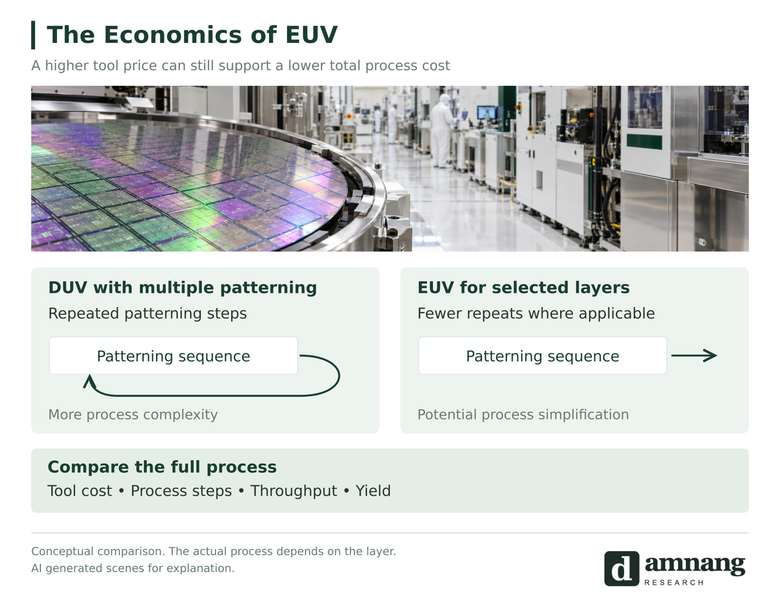
More precisely, the economics justify adopting it. Multiple patterning with DUV can create smaller patterns, but it requires repeating process steps. That means more equipment and more time for a wafer to move through the process. More difficult alignment can also affect yield.
An EUV system may look expensive when you consider its purchase price alone. But if using it reduces the subsequent process steps and the amount of equipment needed, it can be more economical overall. Ultimately, you are comparing how much of the same output you can produce and at what cost.
I see the widespread adoption of EUV by chipmakers as evidence that it offers these economic benefits in the processes where they use it. That said, I do not know individual customers’ detailed experimental results or the conditions of their process comparisons. Rather than saying that a particular system becomes mandatory at a certain node, you need to consider which approach is more advantageous for the pattern and process in question.
Damnang
When comparing equipment prices, you also need to consider how many wafers each system can process per hour?
Expert
Yes. Throughput is important alongside the equipment price. You need to look at how many wafers the system can process per hour. If the price doubles while throughput stays the same, that price difference remains a cost burden. If throughput is also lower, the difference in cost per wafer can become even larger.
DUV, conventional EUV and High NA EUV systems have different prices. However, any precise price ratios I give here are from memory, so they should be checked against public information. The important point is that you need to compare throughput and repeated process steps along with the purchase price.
Editor’s note In the original conversation, the expert recalled a price difference of roughly ten times between EUV and the latest immersion DUV systems, then added that the figure needed to be checked. Since no specific equipment models or configurations were identified, that ratio is not presented as an established figure in the main text. ASML’s public financial results also group conventional NXE and High NA EXE systems together under EUV. Average revenue for a product category should not be interpreted as the price of an individual system.
3. What High NA Improves and What It Requires
Damnang
How can High NA print finer patterns while using the same EUV wavelength?
Expert
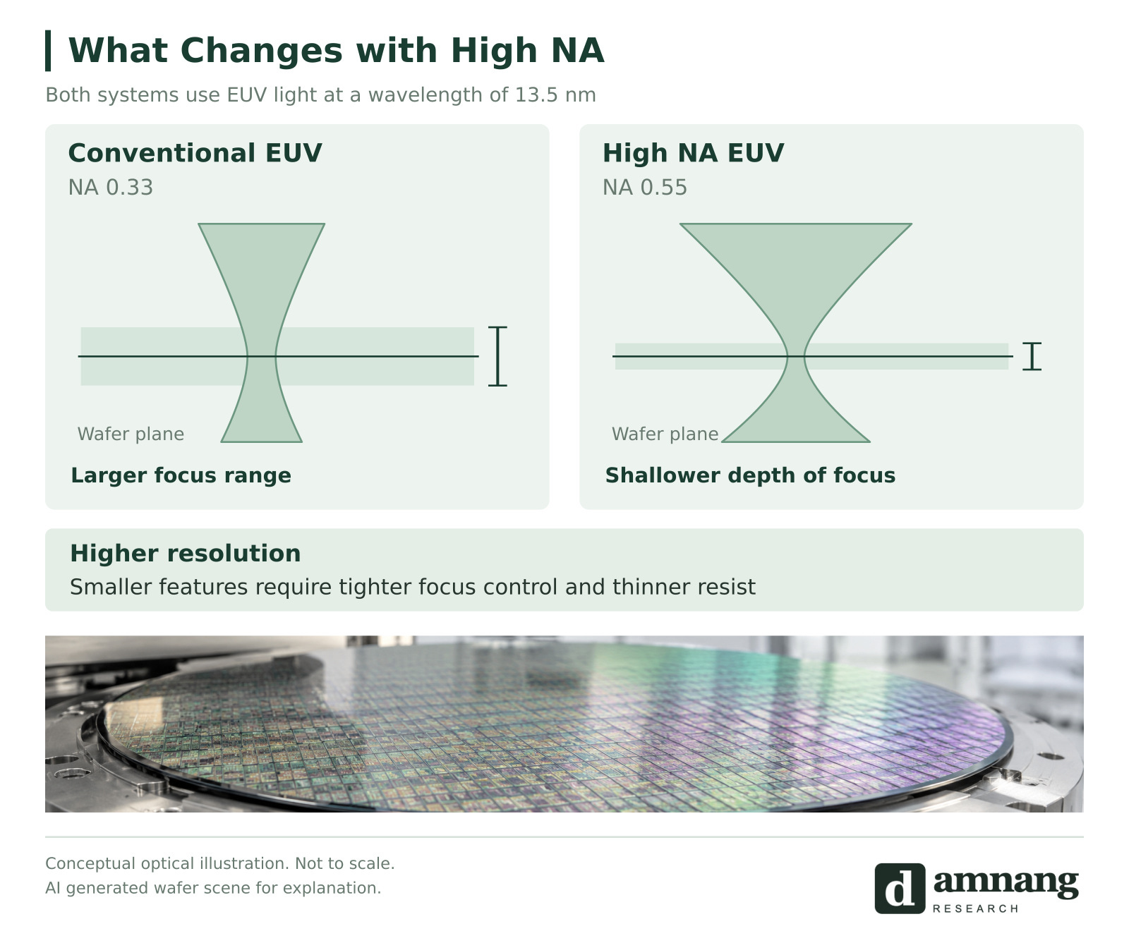
NA stands for numerical aperture. Even at the same wavelength, you can create finer patterns if the optics can focus the light into a smaller area. High NA increases that numerical aperture.
But as you focus the light more tightly, the range of depth over which it stays in focus becomes narrower. Resolution improves, but controlling the depth over which the light interacts with the photoresist becomes more difficult. That creates challenges such as making the photoresist thinner and controlling focus more precisely. Better optics do not mean that all the other process conditions can stay the same.
Editor’s note ASML’s conventional EUV systems use an NA of 0.33, while its High NA EUV systems use an NA of 0.55. Both use a wavelength of 13.5 nm. Increasing NA improves resolution but reduces the depth of focus.
Damnang
Do customers compare multiple patterning with conventional EUV against a single exposure with High NA to determine which is more economical?
Expert
Yes. The same economic logic applies as in the transition from DUV to EUV. If multiple patterning with conventional EUV is more advantageous, customers will use that approach. If forming the pattern in one exposure with High NA is more economical overall, they will move to that instead.
That is why it is important for customers to experiment with the actual equipment. They need to determine whether the benefits of fewer process steps, together with throughput and yield, justify the more expensive system. I believe the point will come when there is an economic case for adopting High NA, and I do not think that point is very far away. But I cannot say exactly at which node every customer will make the transition.
Damnang
Should we think of Hyper NA, which is being discussed as a step beyond High NA, as a continuation of the same approach?
Expert
Reducing the wavelength further is very difficult. That is why increasing numerical aperture while keeping the wavelength unchanged is part of the roadmap. ASML has been working to persuade the industry to move in that direction.
However, I do not have the same level of confidence in High NA and Hyper NA. I believe High NA adoption will eventually expand, but I am not yet sure whether Hyper NA will be economically justified. I think much will depend on how far its cost can be reduced.
Damnang
Lower costs should make the next generation easier to adopt. Why is the comparison with existing equipment still difficult?
Expert
Different generations of equipment share some components. If Hyper NA becomes less expensive because the cost of those components falls, conventional EUV and High NA may benefit as well.
In other words, the next generation may not be the only one getting cheaper. The existing equipment it is compared against may also become cheaper. The next generation then needs to offer an economic advantage even against that lower cost. That is why I would not assume that Hyper NA will necessarily see the same pattern of adoption.