

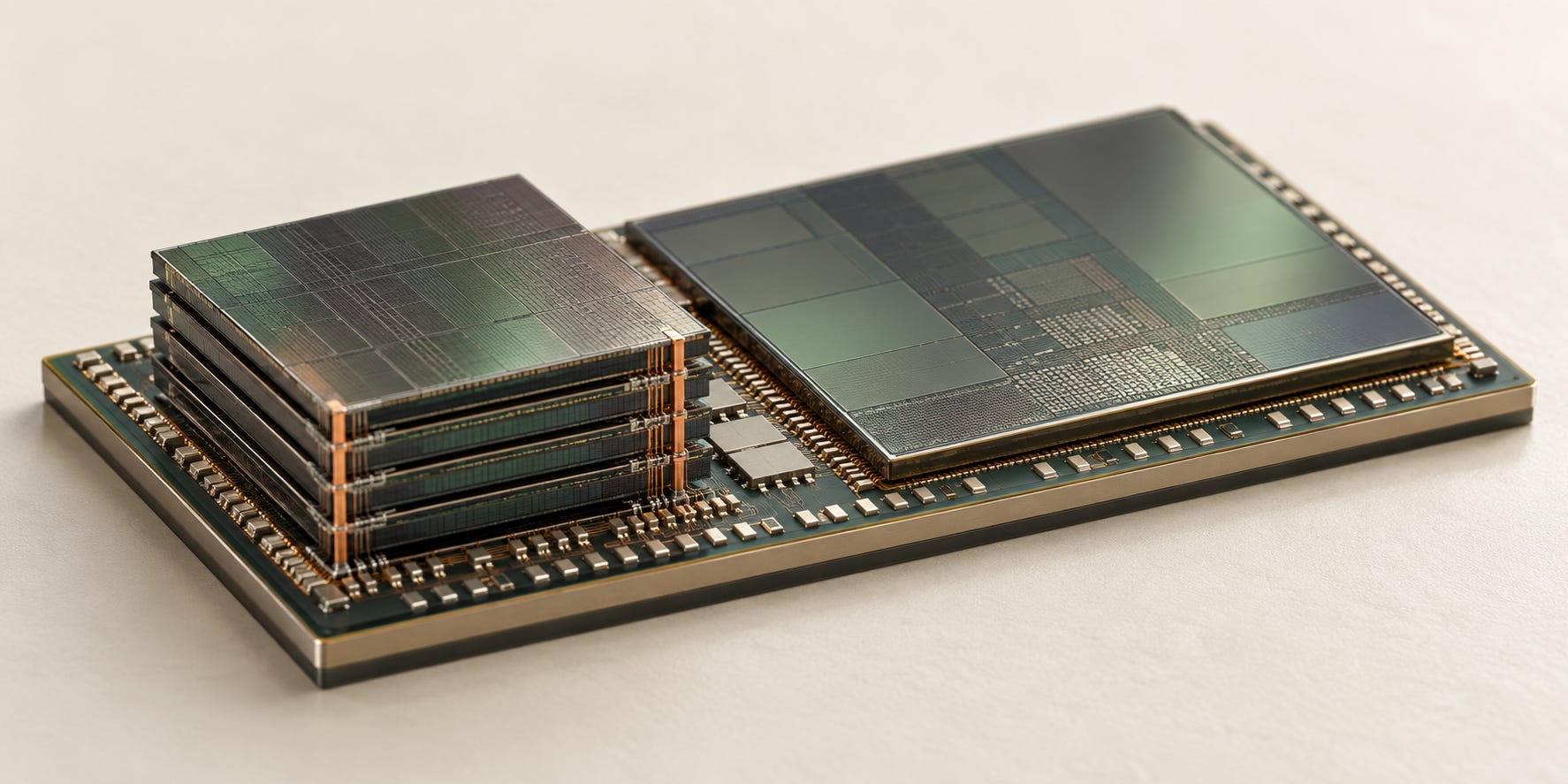
The importance of HBM bandwidth is now familiar. But what has to change inside HBM to make each pin faster? I wanted to understand whether a faster logic process would be enough, whether more TSVs were needed, and how the DRAM stacked above the base die could keep up.
The expert I spoke with designs HBM interfaces at Micron. After working on high speed interface design at Samsung, he moved to Micron, where he now works on both sides of the HBM base die: the interface to the GPU and the interface to the DRAM core dies. Our conversation began with the circuits that transmit and receive signals, then moved into bandwidth and heat in future HBM generations, custom designs, and architectures that stack memory directly on top of a compute chip.
What stayed with me most was how my own question had changed by the end of the conversation. I began by asking what it would take to make HBM faster. As we went on, I became more interested in who would design each part of this increasingly complex memory, and who would capture the value.
I had assumed that bringing memory and logic closer together would naturally expand the role of memory companies. The expert pointed to another possibility. If customers take on more of the logic and interface design, memory companies could end up with a narrower design role even as stacking technology advances. The Q&A below preserves the explanations and followup questions that led me to that realization.
KEY TAKEAWAYS
1. Pin speed is also a problem inside the DRAM.
Distributing incoming high speed data across more internal paths running at lower speeds can ease the demands on DRAM. The cost is more TSVs, more routing, more area, and greater expense.
2.Future HBM makes both receiving and routing harder.
Higher pin speeds increase channel loss and make signals harder to distinguish. If DRAM speed remains unchanged, the design must also accommodate more parallel paths.
3.Fewer layers do not tell the whole capacity story.
Electrical loading, supply conditions, and each customer’s product configuration all matter. Requests for fewer layers do not, by themselves, mean that the need for taller stacks has disappeared.
4.Progress in 3D stacking does not guarantee design control.
Reducing external connections does not eliminate the need to reconcile the speeds of logic and DRAM. If customer specific TSV layouts also require changes to the core die, design reuse and staffing become additional concerns.
The questions and answers have been organized by topic from the original recording. Repetition and personal conversation have been removed; this is not a verbatim transcript. The context distinguishing the expert’s experience, information heard from others, and personal reasoning has been preserved. The answers do not represent the company’s official position. Explanations added beyond the interview are labeled “Editor’s note,” and the interviewer’s analysis is labeled “Damnang’s take.”
Generative AI assisted with editing and the creation of visual material.
1. HBM has two distinct interfaces
Damnang
Could you start by briefly introducing the work you do?
Expert
I design HBM at Micron, specifically the interfaces. An interface enables chips to exchange signals reliably. Our job is to transmit clean signals, receive them without errors, interpret the incoming analog signals as digital data, and pass that data into the chip.
I specialized in high speed interface design during my PhD and also worked on SSD interface design at Samsung. I later moved to Micron, where I now design HBM interfaces.