Semiconductor design might sound like an intimidating, highly specialized field, and honestly, it is. It’s not easy to approach without an electrical engineering background.
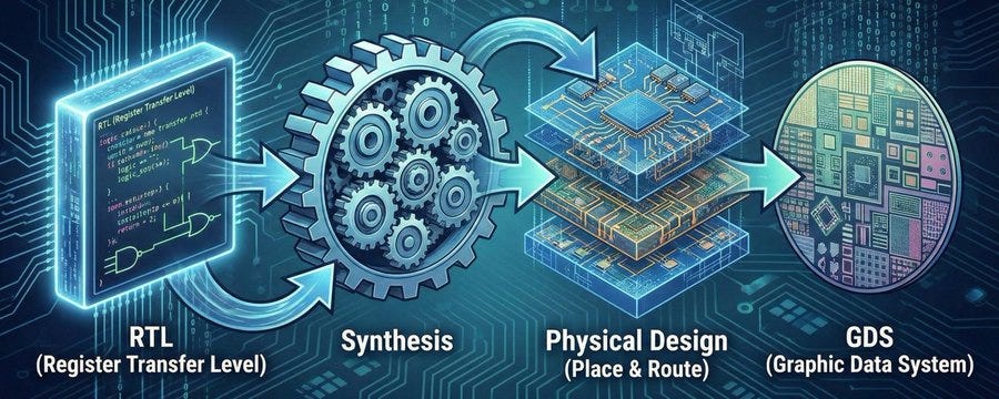
In this article, I’ll walk you through the entire process of how a chip is made, from transistors to the final design file (GDS). This is what we call RTL2GDS in the industry. My goal is to explain it in a way that even non-engineers can follow. After reading this, I hope you’ll have a better understanding of the big picture of semiconductor design and be able to make more sense of semiconductor news in the future.
Substack is currently in a trial phase, so all premium quality articles are available for free for now. Once paid subscriptions are introduced, pricing will be set at a level comparable to professional tech writers on Substack. Early supporters will have the benefit of locking in their current pledge price for future paid access.
1. Transistor
What is a Semiconductor?
Let’s start with the name itself. A conductor is a material that conducts electricity well, and an insulator doesn’t conduct at all. A semiconductor is somewhere in between—it normally doesn’t conduct electricity, but under certain conditions, it can.
Silicon is the most common semiconductor material. Pure silicon doesn’t conduct electricity well, but when you add impurities (a process called doping), its electrical properties change. This is the principle behind the transistor.
The structure of a transistor is incredibly complex, but here’s all you need to understand: A transistor is a switch that controls the flow of current using electrical signals.
Apply voltage to the Gate → Switch ON (current flows)
No voltage at the Gate → Switch OFF (current blocked)
Billions of these tiny switches packed together create the CPUs and GPUs we use every day. (Of course, there’s much more inside a chip than just transistors.)
Why Digital Uses 0s and 1s
Once you understand that a transistor is a switch, it becomes clear why digital circuits use binary (0 and 1). A switch has only two states: ON or OFF. Represented as numbers, that’s 1 and 0.
Using a transistor in some “half-on” state would make it susceptible to noise and unstable. So we stick to definite ON/OFF states. In other words, the 0s and 1s in digital circuits aren’t a philosophical choice—they naturally emerge from the physical characteristics of transistors.
What Do 3nm and 5nm Mean?
You’ve probably heard news about “Samsung’s 3nm process” or “TSMC 5nm.” These numbers roughly indicate the size of transistors. Smaller numbers mean smaller transistors, which means more transistors can fit in the same area. More transistors enable more complex computations, and smaller transistors consume less power.
(Note: Recently, numbers like 3nm and 5nm don’t represent exact physical dimensions—they’re more like generation names for each company’s process technology.)
Evolution of Transistor Structures: FinFET and GAA
You may have also heard terms like FinFET and GAA in the news. These are all types of transistors, just with different structures. While the technology behind them is complex, here’s the simple takeaway:
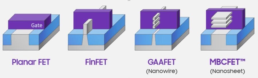
Transistors evolved from Planar → FinFET → GAA, enabling precise current control even at smaller sizes.
See Appendix A below for a brief explanation of transistor structures.
2. Gate: Building Logic from Transistors
I mentioned that transistors are switches that can represent 0 and 1. By combining multiple transistor switches, we can create circuits that perform logical operations. We call these Gates.
Basic Gates
NOT (Inverter): Flips the input.
AND: Outputs 1 only when both inputs are 1.
OR: Outputs 1 when at least one input is 1.
By combining these three, we can create other gates like XOR (outputs 1 when inputs differ), NAND (opposite of AND), and NOR (opposite of OR).
Building an Adder with Gates: 1-bit Half Adder
“What can you actually do with AND and OR?” you might ask. Let’s look at a simple example: the 1-bit Half Adder.
It takes two 1-bit inputs (A and B) and outputs their Sum (S) and Carry (C).

Finding the gate combinations that satisfy this truth table:
S: Outputs 1 when A and B differ → XOR characteristic → A XOR B
C: Outputs 1 only when both A and B are 1 → AND characteristic → A AND B
Using the properties of logic gates, we can implement virtually any computation.
PDK and Standard Cell Library
Here are some important concepts:
PDK (Process Design Kit): A package of process information provided by the foundry. It contains information about how to build transistors in a specific process (e.g., TSMC N3).
Standard Cell Library: A library of pre-designed gates built on the PDK. It includes cells like AND, OR, NOT, XOR, and Flip-Flops, along with their timing, power, and area characteristics.
Here’s the key point: Design companies must decide which foundry’s PDK to use before starting the design. If you start designing with TSMC 3nm PDK, that design can only be manufactured in TSMC’s 3nm process. Switching foundries mid-design means different PDKs, libraries, and design rules, resulting in massive redesign and re-verification costs.
This is why foundry selection is a critical strategic decision that must be made early in the design process. Some companies use a dual-vendor strategy, designing for both foundries simultaneously with different PDKs.
3. Flip-Flop and Clock: Memory and Synchronization
Gates alone have limitations. Combinational logic like AND and OR produces outputs that change immediately when inputs change. In other words, they can’t store values.
Why do we need to store values? Consider calculating (3 + 5) × 2:
Calculate 3 + 5 = 8
Store 8 somewhere
Calculate stored 8 × 2 = 16
Without step 2, sequential calculations would be impossible. The component that temporarily stores values is called a register, and the basic unit of a register is the Flip-Flop.
Flip-Flop (FF): A Circuit that Remembers 1 Bit
A FF is a 1-bit storage circuit made by combining gates. The most commonly used D Flip-Flop includes clock synchronization logic and is typically built from several NAND gates.
Clock: The Signal that Tells FFs When to Store
A clock is a signal that regularly alternates between 0 and 1. FFs capture and store input values when the clock transitions from 0 to 1 (or 1 to 0). All FFs across the entire chip are synchronized to the same clock.
When you buy a computer, you see specs like “3.5GHz” or “5GHz”—that’s the clock speed. 1GHz means the clock ticks 1 billion times per second. Each tick, FFs store values and move to the next operation. Faster clocks mean more operations in the same time. This is why “higher CPU clock = better performance.”
(Of course, these days performance doesn’t scale linearly with clock speed alone, but it remains a key performance metric.)
4. Architecture: What Kind of Chip to Build
Now that we understand transistors, gates, and FFs, let’s talk about actual chip design.
The first decision is: “What kind of chip are we building?” A CPU? GPU? An AI accelerator ASIC? This is called Architecture design.
The same transistors and gates can produce completely different chips depending on how they’re arranged and connected.
IP (Intellectual Property)
In modern chip design, almost nothing is built from scratch. Commonly used circuit blocks are licensed from proven designs. We call these IP (Intellectual Property).
Major IP Companies:
ARM: Dominant in CPU architecture. Most smartphone chips are ARM-based.
Synopsys: Full lineup including USB, PCIe, CXL, DDR, HBM, die-to-die.
Cadence: Strong in PCIe/CXL PHY, USB, DDR IP.
Rambus: HBM, DDR, GDDR, PCIe, and CXL.
Alphawave Semi: High-speed SerDes, PCIe, CXL, UCIe.
SiFive: Commercial RISC-V core IP.
5. RTL Design: Describing Circuits in Human-Readable Language
Once the architecture and specs are defined and necessary IPs are secured, actual design begins.
Why RTL Design Instead of Gate Design?
The 1-bit adder only needed 2 gates. But modern CPUs contain hundreds of millions of gates. It’s impossible for humans to design at the gate level.
So we design at a higher abstraction level called RTL (Register Transfer Level). Instead of individual gates, we describe “how data moves and transforms between registers.”
RTL design uses HDLs (Hardware Description Languages) like Verilog or VHDL. They look similar to software code but actually describe circuits.
Here’s a simple example—a 4-bit counter that cycles 0→1→2→...→15→0 with each clock tick:
verilog
module counter_4bit (
    input        clk,
    input        reset,
    output reg [3:0] count
);

    always @(posedge clk) begin
        if (reset)
            count <= 4'b0000;
        else
            count <= count + 1;
    end

endmodule
count <= count + 1: Add 1 to the current value and store it.
This single line describes: “Every clock tick, the FF stores the value and adds 1.” We didn’t specify which gates to use or how to connect the FFs. That’s determined in the next step: synthesis.
6. Synthesis: Converting RTL Code to Gates
Synthesis transforms RTL code into actual gate connections (netlist). It’s similar to how a compiler converts source code to machine code.
What the synthesis tool does:
Parse Verilog code to extract logic expressions
Optimize the logic (fewer gates, faster speed)
Map to actual gate cells from the Standard Cell Library
Once you describe the circuit specs at the RTL level, the synthesis tool automatically constructs the circuit using verified cells from the library. This makes complex design manageable.
The output of synthesis is a netlist, a text file describing how gates are connected:
verilog
DFFX1  count_reg_0 (.D(n1), .CK(clk), .Q(count[0]));
DFFX1  count_reg_1 (.D(n2), .CK(clk), .Q(count[1]));
XOR2X1 U1 (.A(count[0]), .B(count[1]), .Y(n3));
AND2X1 U2 (.A(count[0]), .B(count[1]), .Y(n4));
7. Physical Design: Placing on the Actual Chip
From a chip design perspective, the netlist still only contains “logical connection” information. The process of physically implementing this on an actual chip is Physical Design. Everything before this is typically called front-end design, while Physical Design onwards is called back-end design.
Physical Design consists of several stages:
Floorplan
Just like deciding where to put furniture when decorating a room, chip design starts with Floorplan. This stage determines the overall chip size and where major blocks will be placed.
Determine total chip area and shape
Decide I/O pin locations
Place macros (memory, analog blocks, etc.)
Design power (VDD, GND) grid
Placement
After Floorplan, the Placement stage positions the synthesized gates on the chip. This optimizes where to place millions to billions of cells.
Place highly connected cells close together
Minimize distance for timing-critical paths
Balance density—not too dense, not too sparse
Congestion management is critical here. If too many cells cluster in one area, there won’t be enough space for routing later. Placement must predict congestion and distribute cells appropriately.
CTS (Clock Tree Synthesis)
This is a crucial stage. Modern chips have tens of millions of FFs, all connected to the clock. But clock signals take time to travel through wires. If FFs on opposite ends of the chip receive the clock at different times, the circuit can malfunction.
CTS designs the clock routing so that clock signals arrive at all FFs on time as originally intended.
Add buffers to maintain signal strength
Adjust wire lengths to match delay times
Distribute via tree structure to minimize clock skew (arrival time differences)
The clock is the chip’s heartbeat—if CTS fails, nothing works. It’s one of the most challenging stages in Physical Design.
Routing
Finally, the Routing stage connects gates with metal wires.
Use multiple metal layers to route without overlap
Minimize signal interference (crosstalk)
Meet timing requirements
Find alternate paths around congested areas
Modern chips use more than 10 metal layers. 3D routing is necessary to handle billions of connections.
What About Analog/Custom Design? The flow described above is for digital design. But chips also contain analog circuits—PLLs (Phase-Locked Loops), ADC/DACs, SerDes analog frontends. These analog circuits can’t be auto-synthesized with Standard Cells; designers must manually place each transistor. Cadence Virtuoso is the de facto industry standard for this custom layout work. If you are interested with ‘analog design’, please refer to the below article.

GDS: The Final Output
When all these processes are complete, a GDS (Graphic Data System) file is produced. This is the final design file containing all layer information for the chip.
The design company sends this GDS file to the foundry (fab) to manufacture the actual chip according to the process specifications. Delivering the final design file to the foundry is called Tape-out. When a semiconductor company announces “Tape-out complete,” it means design is finished and manufacturing has begun.
8. EDA: Essential Design Tools
All the processes described above require specialized software. These are called EDA (Electronic Design Automation) tools.
The Big Three:
Synopsys: Industry leader. Design Compiler (synthesis), ICC2 (PnR), VCS (simulation), PrimeTime (timing analysis), etc.
Cadence: #2. Genus (synthesis), Innovus (PnR), Xcelium (simulation), Virtuoso (analog design), etc.
Siemens EDA (formerly Mentor Graphics): Questa (simulation), Calibre (verification), Tessent (DFT), etc.
These three companies virtually monopolize the semiconductor design tool market. EDA tool licenses can cost tens of millions of dollars annually, which is one reason small startups struggle to enter chip design.
9. Foundry and Manufacturing Process
When the foundry receives the GDS, it goes through complex semiconductor manufacturing processes to produce the chip:
Photomask creation (glass plates with circuit patterns)
Lithography on wafer (transferring patterns with light)
Hundreds of etching, deposition, and other process steps
Dicing the completed wafer (cutting into individual chips)
Packaging (protecting the chip and creating external connections)
Testing and shipment
How Do We Actually Test Semiconductors?

Have you ever wondered how semiconductor testing actually works?
Summary and Conclusion
This article explained the entire semiconductor design process from transistors to GDS. In the industry, we call this process RTL2GDS.
The actual process is far more complex than what I’ve described, but I hope this gives non-engineers a general understanding of the semiconductor design flow. If there’s an opportunity, I’d like to cover specific design technologies, manufacturing processes, or packaging in future articles.
Thank you for reading.
Appendix A: Transistor Structures
Planar FET (Field-Effect Transistor): As transistors kept shrinking, problems emerged. Traditional planar transistors below 20nm suffer from severe current leakage and Short Channel Effects where the Gate can’t properly control the channel.
FinFET (Fin Field-Effect Transistor): First commercialized by Intel at 22nm in 2011. The channel is raised into a vertical “fin” shape, with the Gate wrapping around three sides of the fin. More gate coverage means better current control and reduced leakage. FinFET has been used down to 5nm.
GAA (Gate-All-Around): FinFET hits its limits below 3nm. As fins get too thin, resistance increases, and the bottom of the fin—where the Gate doesn’t reach—still causes leakage. GAA uses horizontally stacked nanosheets as channels, with the Gate completely surrounding all four sides. Samsung introduced GAA at 3nm, and TSMC and Intel are transitioning to GAA at 2nm.