At Google Cloud Next ‘26, held in Las Vegas on April 22, 2026, Google unveiled its 8th-generation TPU.
The most striking change is that the 8th-gen TPU is now clearly split into TPU 8t for training and TPU 8i for inference.
Earlier generations had use-case-specific optimizations like v5p and v5e, but presenting training and inference as two main axes within the 8th generation is a meaningful shift.
The more important thing, though, isn’t the TPU itself.
With this announcement, Google laid out how AI data center infrastructure operates under the name AI Hypercomputer. The AI Hypercomputer concept itself has existed since 2023 and gets updated each year at Cloud Next, but this was the broadest announcement so far, with every part of the infrastructure moving to the next generation at the same time.
For reference, when Google officially explains AI Hypercomputer, it splits into 3 layers:
(1) Performance-optimized hardware (compute, networking, storage)
(2) Open software (framework, OS, orchestration)
(3) Consumption options (provisioning model).
That’s the breakdown when the user receives it as a cloud service. But to analyze the infrastructure itself, you have to look separately at how the accelerators inside the hardware, the host CPU, IPU, memory, communication, data path, storage, and physical infrastructure all operate, and where the bottlenecks emerge. In this article I’ll re-divide it into 6 layers in my own way, which is easier to follow.
This is a different cut from Google’s official categorization.
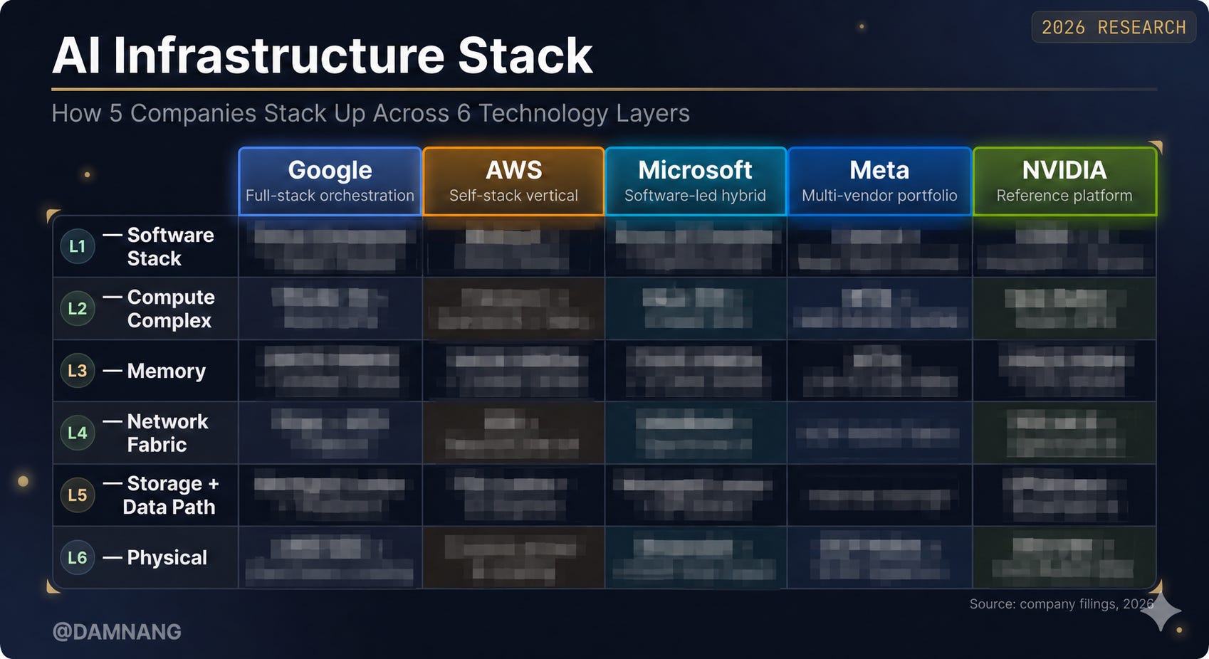
This article walks down from the top layer to explain the entire AI infrastructure structure as Google sees it. Then it places other hyperscalers like AWS, Microsoft, Meta, and NVIDIA on the same layer-by-layer axis for comparison.
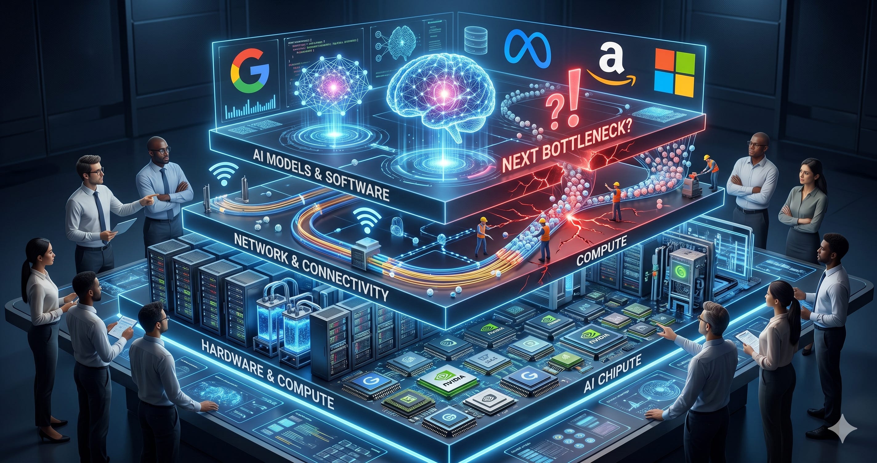
I’ll lay out where standards are aligning at which layer, where bottlenecks emerge that create new investment opportunities, and how the other hyperscalers will repaint this picture in their own colors over the next 24 to 36 months.
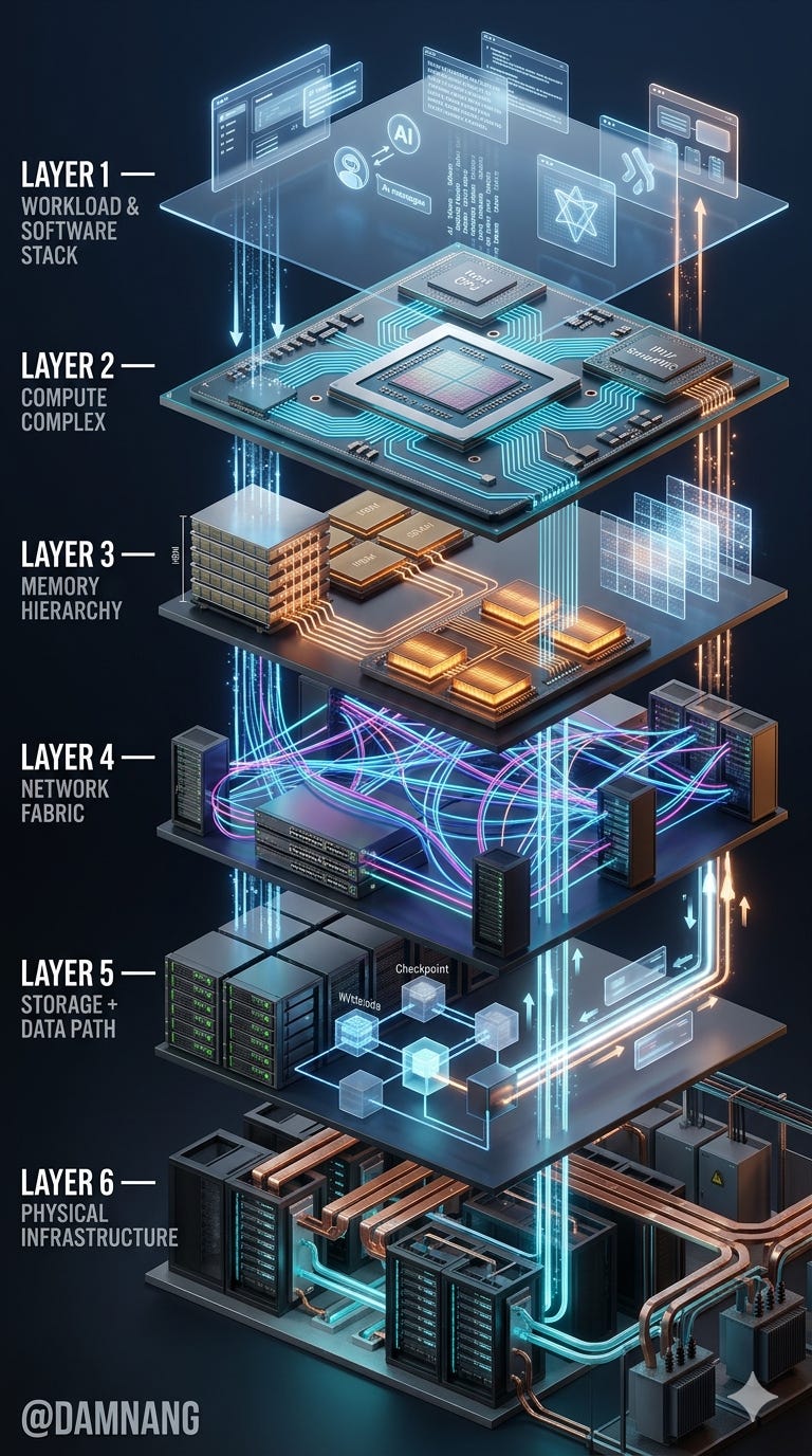
Layer 1. Workload + Software stack: The center of AI work shifts from training to inference
For the past few years, AI infrastructure centered on training. The game was about training larger models for longer, and hardware design followed suit. Compute throughput in a single pass and memory bandwidth. These two were the variables of the game.
Now the center of gravity is shifting to inference. Training is the work of building a model. Inference is the work of using that built model with real users. Training a model once still costs a lot, but in commercial AI services, the cost of inference, which means calling the trained model every day, is becoming an increasingly important variable. As services like ChatGPT and Gemini keep answering questions from users worldwide, costs accumulate not from a single training run but from the inference calls that repeat every day.
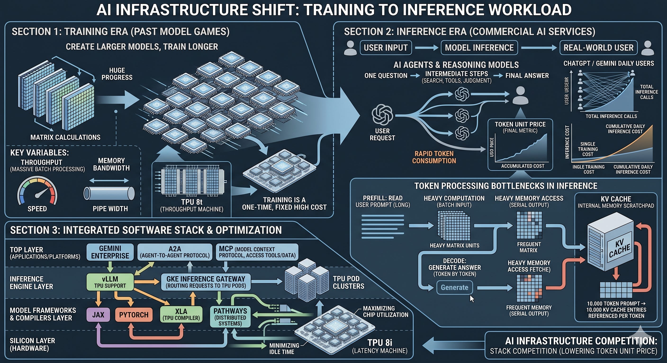
On top of that, with agents and reasoning models going mainstream, a single user request no longer ends with a single line of response. An agent is a structure where the AI takes one user question, runs searches, calls external tools, looks at intermediate results, and judges again, taking multiple steps on its own. A reasoning model doesn’t return an answer right away. It expands its thought process internally over a long sequence and then produces an answer. Both follow a “one question → multiple intermediate processing steps → final answer” structure rather than “one question → one answer,” so the number of tokens the model has to process per user request grows quickly. A token is the unit by which a model processes text. To put it simply, it’s a chunk of a sentence broken into small pieces. One English word, or a few Korean characters or word fragments, can be processed as a single token.
Training and inference demand different things from hardware. Training is a workload that processes large batches at once, so throughput matters. Training chips work best when bundled in the thousands and run for days, pushing massive matrix operations through in one go. Inference, on the other hand, has to produce answers while users wait at their screens, so latency matters. Inference chips work better when designed to repeatedly process short requests fast. That’s why TPU 8t and 8i split the way they did. They’re both 8th-gen TPUs, but the training one is closer to a throughput machine and the inference one closer to a latency machine.
But within inference, the bottleneck isn’t a single thing either. The stage of reading the long prompt the user sent in one go and the stage of generating answer tokens one by one have different characteristics. The first stage is usually called prefill, the second is called decode. Prefill takes the entire user prompt at once and builds the model’s internal state, which is compute-heavy. Decode is the stage that generates answer tokens one at a time from that state, and each token requires referencing all the prior calculation results. So prefill is compute-heavy, and decode is memory-access-heavy.
Here the concept of KV cache enters. As the model processes the prompt, it accumulates intermediate calculation results in memory. This is called KV cache. K stands for key, V for value. Think of it as a kind of notepad the model references when predicting the next token. During decode, every time a new token is created, it has to keep referring back to that notepad. So the longer the user’s prompt, and the longer the answer, the bigger the notepad gets, and the larger the data that has to be read each time. If you put a 10,000-token document in as a prompt, 10,000 tokens worth of KV cache piles up in memory, and each time a single answer token is generated, the model has to keep referencing information equivalent to that 10,000 tokens.
The most important variable at this layer is token cost. AI service costs ultimately accumulate in proportion to the number of tokens the model processes. As inference usage grows, the margins of hyperscalers and AI labs are determined by how cheaply they can process one token. And token cost isn’t determined by chip performance alone. With the same hardware, actual costs vary significantly depending on how the software distributes user requests, how well it manages KV cache, and how busy it keeps the accelerators.
That’s why Google didn’t talk only about chips in this announcement and emphasized the software stack alongside. Software in the inference era isn’t a side feature. It’s closer to a full operations system that takes user requests, connects agents to external tools, distributes work across multiple TPU pods, and translates model code so the TPU can execute it well. To lower token cost, the chip itself has to be fast, but you also need software that keeps that chip fed.
From this perspective, Gemini Enterprise, A2A, MCP, vLLM TPU support, and GKE Inference Gateway are software at different layers. Gemini Enterprise is the platform where enterprises connect Gemini models to their own data. A2A is the protocol for multiple AI agents to communicate. MCP is the protocol for AI to access external tools and data. vLLM is an open-source engine that efficiently distributes inference requests across multiple chips, and GKE Inference Gateway is the gateway that routes inference requests across multiple TPU pods. The names differ but the direction is the same. They’re software layers built to handle more inference requests at lower cost.
On top of that, Google didn’t only design the chip. JAX, PyTorch, vLLM, XLA, and Pathways are co-designed with hardware in the same stack. This is part of the same flow. JAX and PyTorch are frameworks for building models, XLA is the tool that compiles that model code into instructions the TPU can understand, and Pathways is the system that distributes a single model across many chips. Making the TPU faster and getting software to feed the TPU properly are the same problem. No matter how fast the chip is, if the software can’t distribute requests properly, only some of the chips work and the rest spend their time waiting on data.
AI infrastructure competition is shifting from a fight to build faster chips to a stack competition to drive down token cost. When workloads change, software changes. When software changes, the hardware design beneath it changes. The split between TPU 8t and 8i is a sign that this shift has reached the silicon.
Layer 2. Compute complex: A compute system bundling accelerator, host CPU, and IPU into one
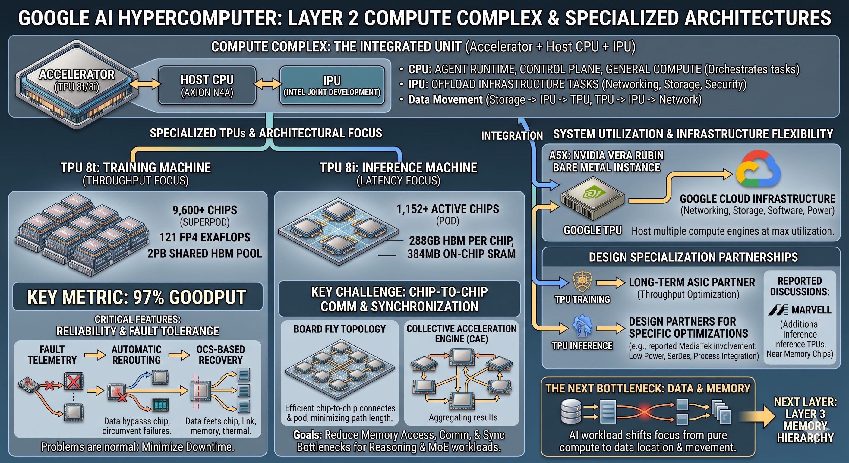
In actual AI data centers, a single TPU chip doesn’t run alone. Next to it sits a host CPU coordinating the work, and an IPU handles networking and storage communication on its behalf. The compute complex, where accelerator, host CPU, and IPU bundle into one, is the real compute system. The foundation of what Google calls AI Hypercomputer also lives here.
In this structure, the most visible part is the TPU. But the TPU is also no longer a chip with a single purpose. Google split the 8th-gen TPU into training and inference variants. TPU 8t is the training chip, TPU 8i is the inference chip. They both look like AI accelerators, but the bottlenecks the two chips target are different.
TPU 8t is the training chip. It bundles 9,600 chips into a single superpod, providing 121 FP4 exaFLOPS of compute and a 2PB shared HBM pool. Training is the work of dividing massive models across thousands of chips and running them for a long time. So beyond individual chip performance, what matters is whether thousands of chips move stably as if they were a single system.
The number I find most important about TPU 8t isn’t peak FLOPS.
It’s 97% goodput.
In large-scale clusters, problems with chips, links, memory, and thermals always erupt somewhere. Failure isn’t an exception, it’s a normal operating condition. The competitiveness of next-generation AI infrastructure doesn’t end with building the fastest chip. The ability to quickly detect failed chips, links, and slowed paths, then route around them while keeping training going, is becoming increasingly critical. Fault telemetry, automatic rerouting, and OCS-based recovery all live here. From my view, this reliability and diagnosis layer is one of the hidden bottlenecks of AI infrastructure.
TPU 8i is the inference chip. It bundles up to 1,024 active chips into one pod, with 288GB HBM and 384MB on-chip SRAM per chip. Inference has to repeatedly process short responses quickly while users wait. Especially in reasoning and MoE workloads, chip-to-chip communication, cache access, and synchronization determine latency. TPU 8i is designed to reduce latency rather than maximize peak compute. The Boardfly topology shortens inter-chip communication distance, and CAE accelerates the work of multiple chips collecting and synchronizing results. The point isn’t more compute. It’s about cutting away the memory-access, inter-chip communication, and synchronization bottlenecks that emerge during inference.
Looking at it this way, TPU 8t is a throughput machine for training that pushes long compute runs, while TPU 8i is a latency machine for inference that processes short requests quickly. When the workload changes, the bottleneck changes. When the bottleneck changes, the silicon design changes too. The split between 8t and 8i is a signal that this shift has reached the chip architecture itself.
But TPU alone doesn’t complete the compute complex. Alongside it sits the Axion N4A host CPU and the next-generation IPU being co-developed with Intel. The host CPU handles agent runtime, the control plane, and general computing tasks. The IPU takes networking, storage, and security work off the host CPU. No matter how fast the accelerator, if the data doesn’t arrive on time, it goes idle. The host CPU and IPU are essential components for keeping accelerator utilization up.
What Google calls AI Hypercomputer isn’t a strategy of just making TPUs faster. It’s a structure where the TPU handles compute, the CPU coordinates work, and the IPU handles data movement and infrastructure tasks, all driving up the utilization of the entire system. The competitiveness of AI data centers now comes not from individual accelerator performance but from how smoothly these components fit together.
The fact that Google also announced A5X at the same event has to be read in this context. A5X is a bare metal instance based on NVIDIA Vera Rubin. This is closer to a strategy of running both Google’s own TPU and NVIDIA GPUs inside Google’s cloud, rather than a strategy of completely replacing NVIDIA with TPU. Whether the customer uses TPU or NVIDIA, the networking, storage, software, and power infrastructure beneath them runs on Google Cloud. Google’s real strategy isn’t a specific chip. It’s running multiple compute engines inside its own infrastructure at the highest possible utilization.
The design partner setup here is also interesting. The training TPU appears to continue with Google’s long-time ASIC design partner, while MediaTek is reported to be involved in the inference TPU according to Bloomberg and The Information. There’s no official announcement, but the direction itself matters. MediaTek brings low-power design experience, SerDes capability, and TSMC process integration accumulated from mobile SoCs. Inference chips need cost, power, and latency optimization more than training chips do. If Google is moving toward not putting all TPU designs through one channel and instead using different partners by workload, that’s a signal that AI accelerator design is becoming more segmented.
The Information also reported that Marvell is in discussion with Google not only for additional inference TPUs but also for assistant chips that sit alongside the TPU and reduce memory bottlenecks. Neither company has officially confirmed. So this part is safer to read as a signal of Google’s multi-vendor design direction rather than a confirmed supply chain.
What to look at in this report is the memory bottleneck. In AI workloads, the bigger and bigger bottleneck isn’t compute itself. It’s where the data sits, how it’s brought in, and how often it gets moved. If you can process some compute near memory or reduce the data movement itself, another axis emerges for driving up accelerator efficiency. This point connects naturally to the next Layer 3, memory hierarchy.