

Executive Summary
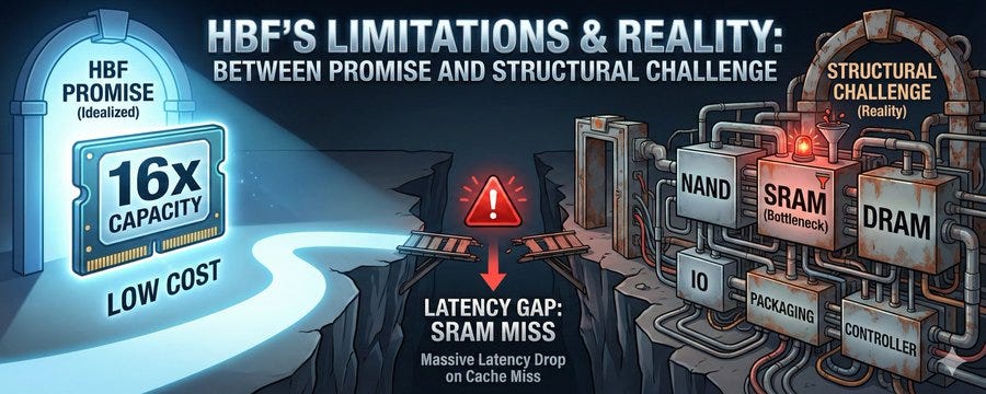
High Bandwidth Flash (HBF) emerged with an ambitious promise to solve AI’s memory bottleneck. The idea was to stack NAND flash like HBM, delivering HBM-level bandwidth with 16x more capacity. SK hynix and SanDisk are developing this technology with a target of sampling in late 2026, and on the surface, it looks like the perfect answer to LLM inference memory capacity problems.
However, a close analysis of the H³ paper published by SK hynix researchers reveals that HBF faces much higher barriers to practical implementation than initially apparent. This article examines the assumptions and limitations of the H³ architecture from a practicing semiconductor engineer’s perspective, reviews the technical and economic challenges HBF will face during commercialization, and looks at alternative technology solutions currently being developed in the industry.
Key findings:
The read-only workload assumptions in H³ are very limited in actual LLM inference scenarios. Overcoming NAND’s fundamental physical limitations (1-2 orders of magnitude latency difference) requires a 40MB SRAM buffer, DRAM, and complex controllers, which undermines the initial promise of “cheap NAND.” Practical barriers like production yield, thermal management, and reliability validation are higher than expected. Alternative solutions like CXL Memory, HBM4, and software optimizations are maturing faster.
1. Background of HBF: The Memory Capacity Crisis Created by AI
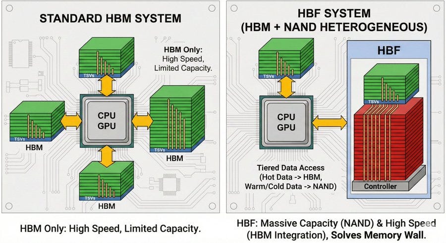
The bottleneck in AI workloads is no longer compute performance. To keep up with the 989 TFLOPS that NVIDIA’s H100 can deliver, memory needs to supply data just as fast. HBM3 meets this requirement with 819GB/s bandwidth and 100ns access latency, but it has a critical weakness: This is capacity. At maximum 192GB per GPU (B200), HBM is woefully insufficient for running large models like Llama 3.1 405B (about 405GB in FP8) on a single GPU.
The bigger problem is KV cache. For Llama 3.1 405B with 1M token context, pre-computed KV cache alone reaches about 540GB. Extending to 10M tokens means 5.4TB. Handling this with HBM alone would require dozens of GPUs, driving up both cost and power consumption proportionally.
This is the background for what SanDisk and SK hynix call the “memory wall” and their proposal of HBF.
HBF’s promise is clear: stack NAND flash with TSV (Through Silicon Via) like HBM to provide 16x the capacity of HBM (~3TB) at equivalent bandwidth (8TB/s). Since NAND costs about 1/5 of HBM, the economics work out too. On the surface, it’s a perfect solution. But we need to look more closely.
2. The H³ Paper’s Approach: Hybrid Architecture and Core Assumptions
2.1 H³ Architecture Overview
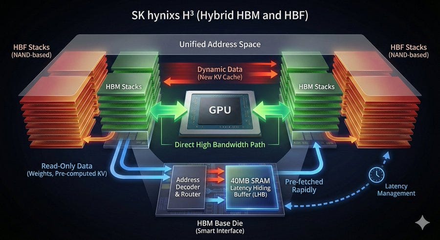
The H³ (Hybrid architecture using HBM and HBF) proposed by SK hynix researchers acknowledges HBF’s limitations when used alone and takes a hybrid approach combining HBM and HBF. The core design works like this:
HBM connects directly to the GPU shoreline for maximum bandwidth. HBF connects through the HBM base die in a daisy-chain configuration. An address decoder and router inside the HBM base die separates HBM/HBF access. A 40MB SRAM-based Latency Hiding Buffer (LHB) mitigates NAND’s slow access latency.
In this structure, the GPU sees both HBM and HBF as main memory through a unified address space. Read-only data (model weights, pre-computed KV cache) goes in HBF, while dynamically generated KV cache stays in HBM.
2.2 Core Assumptions
H³’s performance claims rest on several important assumptions:
Workload assumption: Most LLM inference data is read-only. Model weights and shared pre-computed KV cache don’t change during the entire inference period.
Access pattern assumption: LLM inference is deterministic and sequential. Therefore, needed data can be accurately predicted and prefetched in advance.
Performance assumption: The 40MB SRAM buffer achieves a high enough hit rate (not explicitly stated in the paper, but implicitly requires 80%+ ) so that HBF’s 20μs latency stays hidden most of the time.
Latency hiding assumption: Since LLM inference is memory bandwidth-bound, the hop latency from HBF access can be sufficiently hidden.
Cost assumption: Since NAND dies are cheap, the total system remains economical compared to HBM-only even after adding extra components (SRAM, DRAM, controller, TSV).
The paper’s simulation results are impressive. 1.25x throughput improvement for 1M token cases, 6.14x for 10M token cases. Throughput per power reaches up to 2.69x. Even cutting HBF bandwidth in half still beats HBM-only.
But these results are only achievable when all the above assumptions are met. And that’s where the problem lies.
3. Limits of Assumptions and Technical Feasibility Issues
3.1 Limitations of the Read-Only Workload Assumption
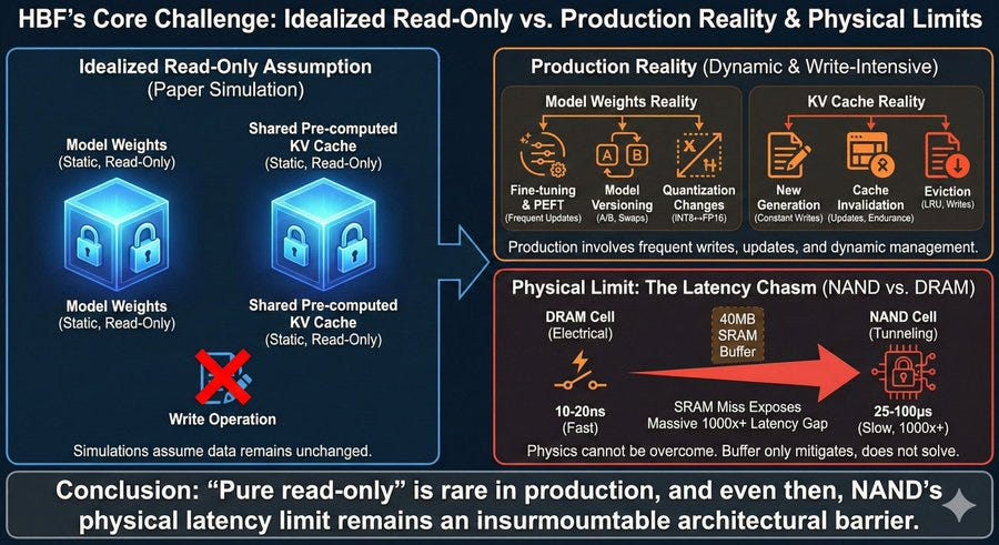
The paper classifies model weights and shared pre-computed KV cache as “read-only,” but how valid is this assumption in actual production LLM services?
Reality of Model Weights:
Fine-tuning and PEFT: In production environments, parameter-efficient fine-tuning like LoRA and QLoRA is common. Adapter weights are small but frequently updated.
Model versioning: A/B testing or gradual rollout scenarios involve serving multiple model versions simultaneously. How does HBF handle model swaps?
Quantization changes: Dynamic switching between INT8, FP8, and FP16 is a common production optimization technique.
Reality of KV Cache:
Scope of pre-computed cache: The cache-augmented generation (CAG) that the paper presents is a valid use case, but it covers only a tiny fraction of total LLM inference. General-purpose conversational services like ChatGPT and Claude generate new KV cache for every request.
Cache invalidation: When shared documents get updated, how do you refresh pre-computed cache? Given HBF’s low write endurance, this is a critical issue.
Cache eviction: Managing hundreds of GB of shared cache pool requires replacement policies like LRU, which involve writes.
3.2 NAND’s Physical Limits: An Unavoidable Wall
Even if the read-only assumption holds, a more fundamental problem remains. The latency difference between NAND cells and DRAM cells isn’t something architectural tricks can solve. This comes from differences in physical laws:
DRAM cell: Reads and writes charge in a capacitor. Only requires electrical switching. 10-20ns.
NAND cell: Moves electrons to a floating gate through tunneling. Requires high voltage and long time. 25-100μs.
That’s a 1-2 order of magnitude difference. This is also the fundamental reason Intel Optane (3D XPoint) couldn’t replace DRAM. Even Optane’s ~100ns latency couldn’t match DRAM’s 10-20ns. HBF’s 20μs? That’s a 1000x difference.
The 40MB SRAM buffer “mitigates” this difference but doesn’t “solve” it. The moment an SRAM miss occurs, that difference is fully exposed.
In other words, “pure read-only” workloads are very limited in practice, and even when read-only is guaranteed, NAND’s physical latency limits can’t be overcome. The paper’s simulation represents an idealized scenario.
4. Cost Structure Reality: The “Cheap NAND” Trap
HBF advocates emphasize that “NAND wafers cost much less than HBM.” True. Looking at just the NAND die itself, it’s definitely cheaper than an HBM die. But what about total cost?
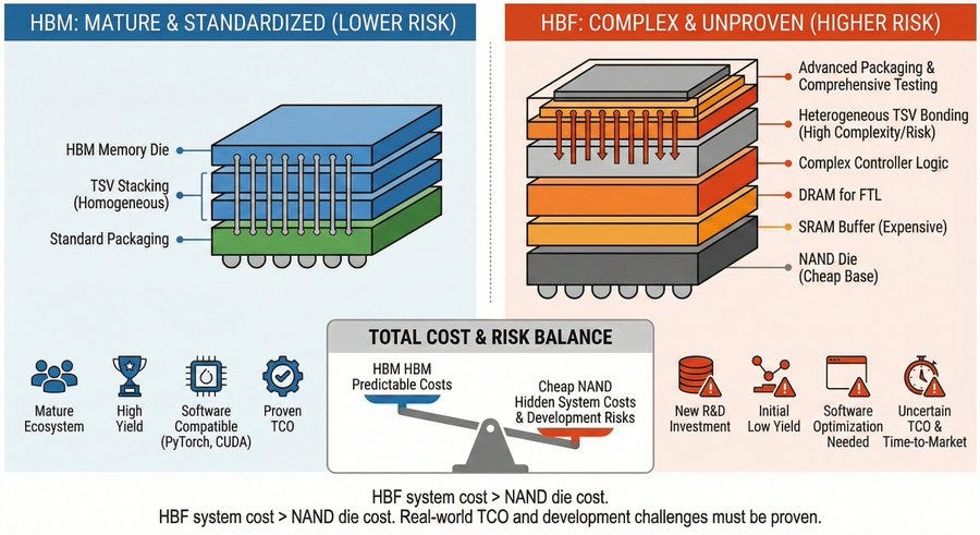
For HBM, the main costs are memory dies, TSV stacking, and packaging. The controller is integrated inside the GPU, and no separate buffer or intermediate layer is needed. The structure is relatively simple.
HBF starts with cheap NAND dies, but it doesn’t end there. To hide NAND’s slow latency requires a 40MB SRAM buffer. This isn’t a small cache memory but a substantial amount of high-speed memory. SRAM costs far more per unit area than NAND.
Add to this the separate DRAM needed to run the FTL (Flash Translation Layer). Like an SSD controller stores metadata, HBF needs working memory for address mapping and wear leveling. This DRAM is an additional cost.
TSV stacking and bonding itself is an expensive process. TSV involves drilling microscopic holes vertically through silicon and filling them with metal. It requires expensive equipment and precise process control, and a single mistake can render the entire die defective. HBM uses homogeneous stacking of identical memory dies, so the process is relatively standardized. HBF uses heterogeneous stacking mixing NAND, SRAM, and controller logic.
Aligning and bonding dies with different characteristics is much trickier. They have different thermal expansion coefficients, different electrical properties, and different reliability requirements. This significantly increases process complexity, leading directly to lower yields and higher costs. Problems like die cracking when drilling TSVs, misalignment during bonding, or delamination from thermal stress become more likely.
Packaging and testing also get more complex. For HBM, memory access testing is the main validation item. For HBF, you need to verify SRAM buffer hit rates, FTL accuracy, wear leveling algorithms, ECC (Error Correction Code) operation, garbage collection efficiency, and more. It’s essentially SSD controller-level complexity.
The cost of the controller logic itself that manages all this can’t be ignored either. HBM is a simple memory interface, but HBF needs a sophisticated controller performing complex address translation, prefetching, cache management, wear leveling, and garbage collection.
More importantly, there’s development cost and risk. HBF is a completely new architecture. It requires massive investment and time for R&D, standardization work, software ecosystem building, and customer validation. HBM has already been through all this. Yields are stable and the ecosystem is mature. HBF has to start from scratch.
Low yields in early production also matter. HBM initially had low yields and high cost per unit. It improved gradually over several generations. HBF uses more complex heterogeneous stacking than HBM, so initial yields will likely be lower. If yield is half, cost is effectively double.
Software integration costs can’t be overlooked either. PyTorch, TensorFlow, CUDA, and all AI frameworks were designed assuming HBM and DRAM. To efficiently use HBF’s SRAM buffer requires optimizing memory allocation strategy, data placement, prefetching hints, and more at the software level. This takes significant engineering resources.
So while “NAND is cheap” is true, “HBF systems are cheap” needs verification. Starting with cheap materials, all the elements added in making it into a practical product drive up total cost. For HBF to prove economic advantage, it needs to demonstrate not just $/GB but actual TCO (Total Cost of Ownership) in real workloads.
5. Alternative Technology Solutions and Market Dynamics
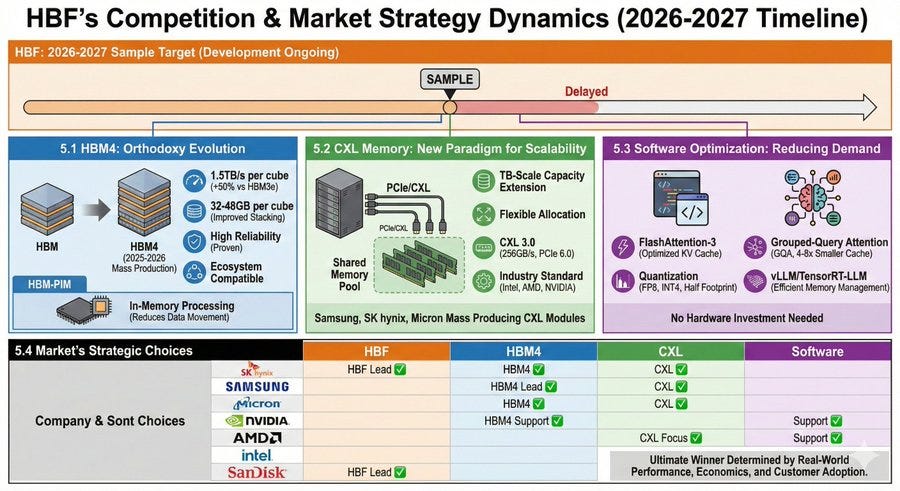
While HBF aims to sample in 2026-2027, other technologies are already maturing rapidly. The industry is approaching the same problem of memory capacity expansion in different ways.
5.1 HBM4: The Power of Conventional Evolution
SK hynix, Samsung, and Micron are focusing on HBM4 development. Production target: 2025-2026.
Bandwidth: 1.5TB/s per cube (50% improvement over HBM3e)
Capacity: 32-48GB per cube (improved stacking technology)
Reliability: Maintains proven HBM reliability
Ecosystem: Perfect compatibility with existing software stack
If 384GB per GPU (8 cubes × 48GB) becomes possible, HBF’s “capacity advantage” shrinks. Plus HBM4 is proven in latency, reliability, and ecosystem.
HBM-PIM (Processing-In-Memory): Samsung’s HBM-PIM performs simple operations (vector addition, activation) inside the memory. It reduces data movement to increase effective bandwidth. More innovative than HBF while building on the existing HBM ecosystem.
5.2 CXL Memory: A New Paradigm in Scalability
Compute Express Link (CXL) is a standard connecting CPU/GPU and memory over PCIe. CXL 2.0/3.0 supports memory pooling:
Capacity expansion: Multiple servers access a shared memory pool. TB-scale scaling possible.
Flexibility: Allocate only what’s needed. Better utilization.
Bandwidth: CXL 3.0 is PCIe 6.0-based at 256GB/s (x16 lane). Lower than HBF, but overwhelming in capacity scalability.
Ecosystem: Intel, AMD, NVIDIA all support it. Industry standard.
Samsung, SK hynix, and Micron are already mass-producing CXL Memory modules. This addresses the “large capacity memory expansion” need that HBF targets, but in a different way.
5.3 Software Optimization: Reducing the Problem Itself
Instead of increasing memory with hardware, approaches to reduce memory usage through software are also developing rapidly:
FlashAttention-3: Optimizes KV cache access patterns to reduce memory bandwidth requirements. FlashDecoding++ cuts latency to 1/3 in long context inference.
Grouped-Query Attention (GQA): Adopted by latest models like Llama 3. Reduces KV cache size 4-8x while maintaining performance.
Quantization: FP8 and INT4 quantization cut memory footprint to half or less. NVIDIA H100/B200 natively support FP8.
vLLM, TensorRT-LLM: Inference engines that optimize memory management. Paged Attention reduces memory waste, continuous batching increases utilization.
These software optimizations reduce memory pressure without hardware investment. By the time HBF reaches production, we might not need that much memory in the first place.
5.4 Different Strategic Choices in the Market
SanDisk and SK hynix are leading HBF development. Interestingly, other major memory vendors chose different technology paths:
Samsung: #1 in HBM market share. Focused on HBM4 and HBM-PIM development. No official HBF announcement.
Micron: Started HBM3e supply. Expanding CXL Memory product lineup. No HBF mention.
NVIDIA: B200, GB200 roadmap adopts HBM3e and NVLink-based memory expansion strategy.
AMD, Intel: Focusing on building CXL ecosystem.
This shows the industry is trying to solve the same “large capacity memory expansion” problem through different technical approaches. HBF is a NAND-based innovative approach, HBM4 is gradual improvement of proven technology, and CXL focuses on system-level scalability. Each company appears to have chosen the optimal strategy based on their technical capabilities and market positioning.
Which approach ultimately wins in the market will be determined by actual production performance, economics, and customer adoption rates.
6. Why HBF Still Matters: Memory Companies’ Platform Strategy
Despite the challenges HBF faces, there’s a fundamental business strategy shift in the memory industry behind why this technology gets attention. Traditionally, memory companies were commodity suppliers. Whether DRAM or NAND, they produced to standardized specs and competed on price for market share. The problem with this model is difficulty in differentiation and low margins.
HBM’s emergence started changing this dynamic. HBM isn’t just a memory chip but a system component that needs tight integration with GPUs. It requires complex engineering for TSV stacking, thermal management, power management, and interface optimization with GPUs. This opened opportunities for memory companies to provide higher value and secure better margins.
HBF is an extension of this trend. Beyond simply supplying memory, it proposes a solution that redesigns the entire memory hierarchy. The HBF system is a complex platform integrating NAND, SRAM buffer, DRAM, controller, and interface logic. This enables memory companies to:
Collaborate with customers at the system architecture level
Extend influence into the software stack (prefetching hints, data placement optimization, etc.)
Create technical differentiation beyond simple price competition
Accumulate IP and know-how to raise entry barriers
Samsung’s HBM-PIM follows the same context. By adding compute functions inside memory, memory companies transform from simple storage device suppliers into part of the computing architecture. Micron’s CXL Memory is similar. It’s a platform solution that changes how server systems manage memory.
From this perspective, HBF’s technical challenges don’t necessarily mean project failure. Even if HBF doesn’t replace HBM in the general AI accelerator market, memory companies gain from this process:
Heterogeneous memory stacking technology
Know-how for using NAND as memory
System-level collaboration experience with GPU/AI accelerator vendors
IP accumulation usable for future platform product development
SK hynix collaborating with SanDisk to develop HBF can be understood in this context. SK hynix dominates DRAM and HBM, while SanDisk dominates NAND. Their collaboration is a strategic move experimenting with memory technology convergence and platformization beyond single product success.
Ultimately, HBF isn’t just “memory with more capacity than HBM” but an example of the memory industry’s efforts to transition from commodity business to platform business. Whether this specific product succeeds or fails in the market, this direction itself matters as a long-term survival strategy for the memory industry.
Conclusion: Technology’s Promise and Reality’s Wall
High Bandwidth Flash started with an attractive promise. HBM-level bandwidth with 16x capacity and cheap NAND cost. It looked like it would solve AI’s memory bottleneck in one shot.
But analyzing the H³ paper from SK hynix researchers in depth reveals the price required to keep that promise:
Physical limits: NAND cell’s 1-2 order latency difference can’t be overcome architecturally. The 40MB SRAM buffer is mitigation, not solution.
Exploding complexity: Adding 40MB SRAM, tens of GB DRAM, complex FTL controller, and difficult TSV stacking to “cheap NAND” makes the total system anything but cheap.
Fragile assumptions: The pure read-only workload and deterministic access patterns that H³ assumes are extremely limited in actual production.
Reliability concerns: Whether NAND’s aging, read disturb, and endurance issues in GPU thermal environments can meet production requirements remains unknown.
Market indifference: With major players silent and alternative technologies maturing quickly, HBF’s market positioning looks unclear.
Does this mean HBF will fail?
No. SanDisk and SK hynix’s technical capabilities are beyond question. They’ll prove this technology works at the 2026-2027 sample stage. But “it works” and “it succeeds” are different questions.
HBF’s future is probably:
A niche solution effective in highly specialized CAG workloads
Special markets where power and capacity balance is critical, like Edge AI devices
A complement targeting “the gap between HBM and SSD,” not an HBM replacement
Technology starts with promise, but must overcome reality’s wall to reach the market. HBF is standing before that wall now.
Disclaimer
This article is a technical analysis based on published papers, technical documents, and general semiconductor industry principles. HBF technology’s final performance and market success can only be judged with post-production empirical data.
This article is not intended as investment advice or evaluation of specific companies (SanDisk, SK hynix, Samsung, Micron, etc.). There is no intention to disparage the technical capabilities and R&D efforts of the mentioned companies.
Technology evolves rapidly. Some content may change due to technical developments after this article’s writing (February 2026). Readers should verify the latest information.