

This article is based on the paper “A 36GB 3.3TB/s HBM4 DRAM with Per-Channel TSV RDQS Auto Calibration and Fully-Programmable MBIST” presented by Samsung Electronics at ISSCC 2026. This is a review written with the author’s permission, explaining the paper’s key points from a reader’s perspective and adding personal interpretation.
Substack is currently in a trial phase, so all premium quality articles are available for free for now. Once paid subscriptions are introduced, pricing will be set at a level comparable to professional tech writers on Substack. Early supporters will have the benefit of locking in their current pledge price for future paid access.
Why Samsung Could Flip the Script on HBM4
Samsung’s HBM4 paper at ISSCC 2026 isn’t just a technical announcement. It’s a blueprint for how the company plans to claw back ground it lost to SK Hynix in the HBM market. In this article, I’ll walk through the key technologies one by one, in a way that’s accessible even if you’re not already steeped in semiconductors or HBM.
Before we dive in, let me quickly cover what HBM actually is. If you already know, feel free to skip ahead.
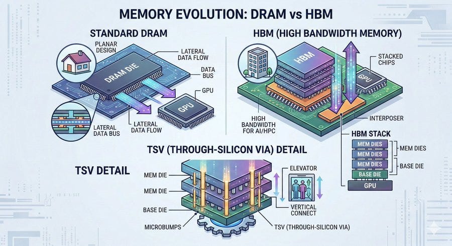
HBM (High Bandwidth Memory) is memory built by stacking multiple DRAM chips on top of each other. If a regular DRAM chip is a single-story house, HBM is a high-rise apartment building. The layers are connected by microscopic vertical channels called TSVs (Through-Silicon Vias) — think of them as the elevators between floors.
The reason we stack chips rather than spread them out is simple: as AI models have grown, the demand for moving massive amounts of data quickly has exploded, and going vertical is far more efficient than going horizontal.
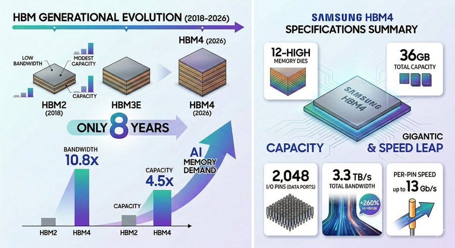
Looking at how HBM has evolved, from HBM2 in 2018 to HBM4 in 2026, bandwidth has grown 10.8x and capacity 4.5x in just eight years. That tells you just how fast AI’s memory appetite is scaling.
Samsung’s HBM4 specs break down as follows: a 12-layer stack, 36GB capacity, 2,048 I/O pins, 3.3TB/s bandwidth (a 260% improvement over HBM3E), and a maximum speed of 13Gb/s per pin. In short — capacity and speed have both taken a massive leap.
One thing worth flagging: the official JEDEC standard for HBM4 (JESD270-4) specifies a maximum data rate of 6.4Gbps per pin, for a total bandwidth ceiling of 2TB/s. Samsung hit 13Gbps in actual testing — more than 2.0x the spec. Even accounting for JEDEC’s deliberately conservative baseline, that tells you just how aggressively Samsung is pushing performance beyond the standard.
If you would like to understand HBM manufacturing across the design, process, test, and packaging stages, please refer to the article below.
Why HBM Is So Hard to Make

HBM is everywhere in the conversation right now. Stock forums, news outlets, casual dinner tables — everyone’s heard that “HBM is in short supply” or “NVIDIA can’t build enough GPUs because of HBM.”
Key #1: Top and Bottom Both Changed — 4nm Logic Base Die + 1c DRAM Core Die
The most fundamental shift in Samsung’s HBM4, as shown in this paper, is a simultaneous generational upgrade to both types of chips that make up an HBM stack.
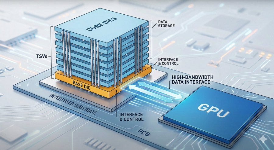
HBM consists of two distinct chip types: multiple core dies (which actually store data) stacked on top of a single base die (which handles the interface with the outside world and serves as the gateway to the GPU).
Start with the base die. Up through HBM3E, even the base die was made on DRAM process technology. DRAM processes are optimized for building memory cells, which makes them relatively limited for implementing complex logic circuits — transistors are larger, and the number of available metal routing layers is constrained. By moving the base die to Samsung Foundry’s 4nm FinFET logic process, transistors shrank dramatically, meaning more circuitry fits in the same area, switching speeds improved, power consumption dropped (VDDQ fell 32%, from 1.1V to 0.75V), and sophisticated logic features like PMBIST and automatic calibration became feasible.
But changing just the base die isn’t enough. That’s where the core die generation jump becomes decisive.
HBM3E’s core dies used a 4th-generation 10nm DRAM process, roughly the “1a” node. HBM4 jumps two generations to the 6th-generation 10nm process, “1c” — skipping 1b entirely. Moving to 1c significantly shrinks the memory cell area, opening up considerably more free space within the same die footprint. Why that free space matters is what the next section is about.
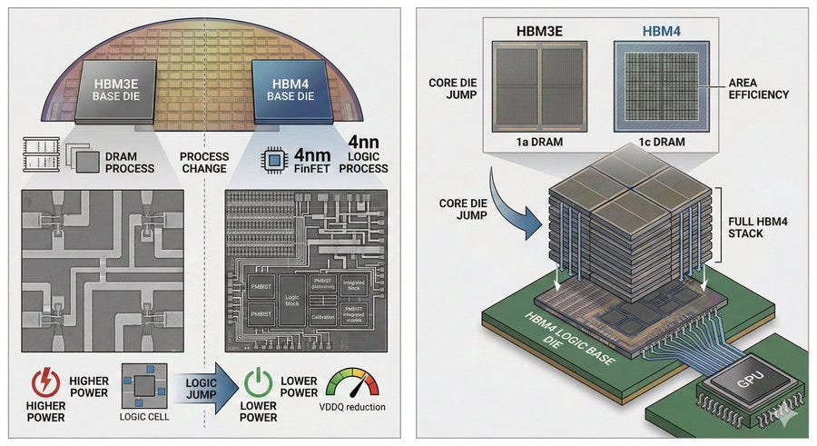
The upshot: Samsung simultaneously moved the base die to 4nm logic and the core die to 1c DRAM, improving area efficiency on both ends. This dual upgrade is what makes everything else in HBM4 possible.
There’s a strategic angle worth calling out here. Samsung owns its own foundry, and 4nm logic is a Samsung Foundry process. Switching the base die to logic is the kind of move that only makes sense if you have memory and foundry capabilities under the same roof. SK Hynix would need to source that logic process externally (e.g., from TSMC). TSMC’s process quality may well be superior, but in terms of vertical integration flexibility and supply security, Samsung’s structure has a real structural edge here.
Key #2: 4x More TSVs and Tighter Microbump Pitch
As explained above, Samsung created area headroom in both the core die (via 1c) and the base die (via 4nm logic). The most direct beneficiary of that headroom is the TSV count.
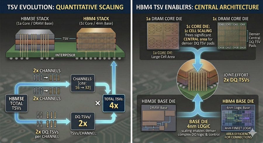
TSVs are the tiny vertical channels that connect the stacked dies and carry data between layers. HBM4 has 4x as many TSVs as HBM3E — channel count doubled (from 16 to 32 channels), and DQ TSVs per channel also doubled. The shrinking cell area of 1c DRAM freed up space to land more TSV pads on the core die, while the 4nm base die provided the matching receiver density below. The paper explicitly credits both sides, describing the 2x DQ TSV increase as a joint product of the 1c core die above and the 4nm base die below.
To explain the relationship between DQ and TSVs: DQ stands for Data Queue — these are the I/O pins through which actual data flows between memory and the outside world. In HBM, DQ signals travel vertically between layers via TSVs. More DQ TSVs means more data can move simultaneously.
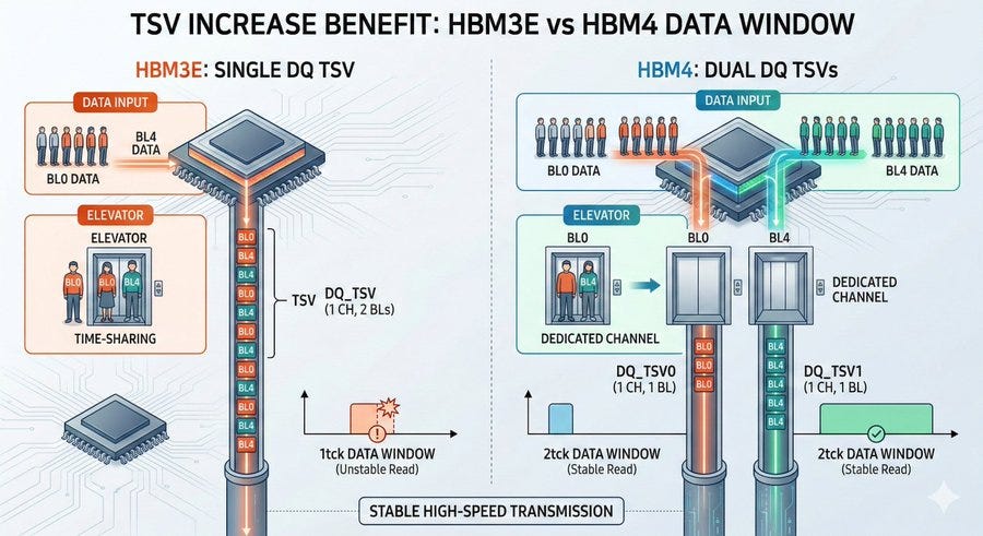
In HBM3E, a single DQ TSV handled both BL0 and BL4 data using time-multiplexing — one TSV alternating between two bit-line signals, like squeezing two passengers into a single elevator car by making them take turns. In HBM4, the two TSVs are split so DQ_TSV0 is dedicated to BL0 and DQ_TSV1 handles BL4. This gives each TSV a 2tck (two clock cycle) data window, versus 1tck in HBM3E. A wider data window means the receiving end has more time to cleanly capture valid data, which is what enables stable high-speed operation.
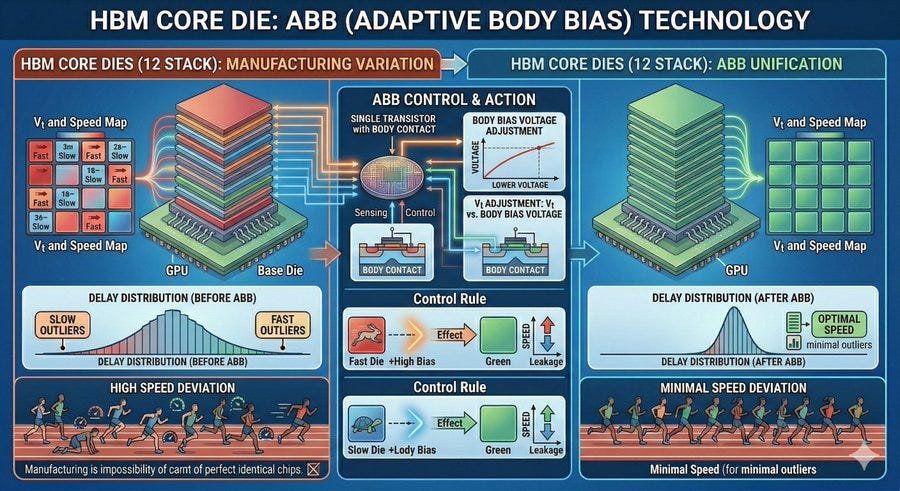
On top of this, ABB (Adaptive Body Bias) technology is applied across the 12 stacked core dies. No two dies are identical — semiconductor manufacturing always introduces subtle variation, and some dies run fast while others run slow. ABB addresses this by adjusting the voltage applied to the body of each die’s transistors, which effectively tunes their threshold voltage (the voltage at which transistors switch on). A higher threshold voltage means slower but leakier transistors; a lower one means faster but with more leakage. By nudging slower dies down and faster dies up, ABB narrows the performance spread across the stack. The paper shows that before ABB, the delay distribution across core dies is wide with notable outliers on both ends; after ABB, the spread tightens significantly.
Key #3: tCCDR Auto Calibration — Solving HBM’s Hidden Performance Bottleneck
The most technically impressive part of the paper is the per-channel TSV RDQS timing auto-calibration. The terminology is dense, but the underlying concept is intuitive. Let me walk through it.
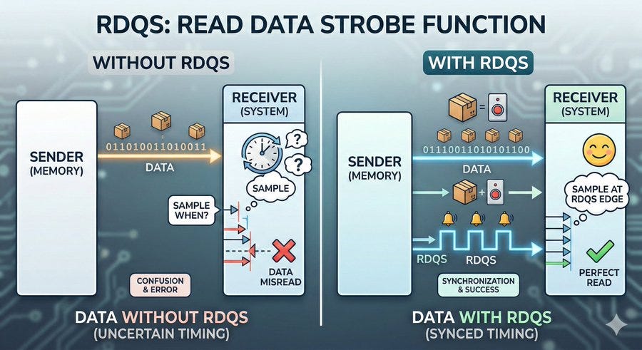
First, RDQS. RDQS stands for Read Data Strobe — it’s the timing reference signal that memory sends alongside data when reading out to the GPU. Without a timing reference, the receiver wouldn’t know when exactly to sample the incoming data. RDQS acts like a doorbell: “Open the door and receive the package right now.” The data is the package; RDQS is the ring of the bell.
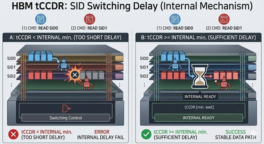
Now, tCCDR. HBM consists of multiple stacked core dies, each with a unique identifier called a SID (Stack ID). When a GPU switches from reading SID0 to reading SID1, there’s a minimum gap required between the two commands. That minimum gap is tCCDR (Column-to-Column Delay for different Ranks) — basically, the minimum wait time required when switching between die layers.
Why does tCCDR matter? AI workloads have the GPU constantly switching between dies at high frequency. A large tCCDR means every die switch incurs a wait, dragging down real-world system performance no matter how fast the per-pin rate is. It’s rarely highlighted in spec sheets, but it’s a parameter that directly affects AI system performance.
The problem in HBM4 — with 32 channels and signals traveling through 12 die layers before reaching the base die — is that tiny timing differences between channels are unavoidable. Some channels have RDQS arriving slightly early, others slightly late. TSV path lengths vary, manufacturing tolerances vary, and temperature and voltage add further drift. From the receiver’s perspective, this is a problem: some channels are “doorbell rang, package safely delivered,” while others are “doorbell still ringing, package still in transit.” If the receiver keeps pushing speed under these conditions, the RDQS-to-data alignment slips in some channels, the valid data window narrows, and errors start appearing.
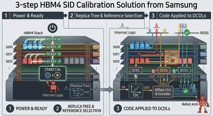
Samsung’s solution works in three stages.
In stage 1, after power-on, the Ready signal from each SID triggers the calibration process.
In stage 2, a reference signal passes through a Replica Tree — a circuit that identically mirrors the actual RDQS signal path, so any timing variation in real operation is accurately reproduced. The slowest SID’s RDQS is selected as the reference, and all other channels synchronize to it.
In stage 3, a TDC (Time-to-Digital Converter) translates each channel’s timing offset into a digital code, which passes through an Offset Controller and Encoder and is applied to each channel’s DCDL (Digitally Controlled Delay Line).
Faster channels get extra delay added; slower channels get less — aligning all channels’ RDQS arrival times.
If that went over your head, here’s a more intuitive version.

Imagine 32 people on a stage, all supposed to clap on the same beat. But everyone’s reaction time is different — one person is consistently 0.2 seconds late, another 0.1 seconds late, another 0.1 seconds early. Without calibration, the conductor has to set the tempo to accommodate the slowest person. Raise the tempo even a little, and the late clappers miss the beat, and instead of a single crisp “clap,” the audience hears a drawn-out scatter of sound. The issue isn’t just one slow person — everyone is off by varying amounts, and the faster the tempo, the more those small gaps become audible.
Now with calibration: before the performance starts, the conductor has everyone do a test clap, measures how early or late each person is, and then tells the faster people to wait — “you, wait 0.05 seconds; you, wait 0.12 seconds.” The idea isn’t to force the slow people faster; it’s to hold the fast people back just enough so everyone arrives at the same moment. Once aligned, the conductor can push the tempo without the claps falling apart, because the offsets have already been corrected.
That’s exactly what Samsung’s calibration does for HBM. The paper’s results are striking: without calibration, the maximum speed at tCCDR = 2nCK was 7.8Gb/s. With calibration applied, it rose to 9.4Gb/s — roughly a 20% improvement. This isn’t just a higher pin speed on paper; it’s a tangible improvement in the performance that an actual AI system experiences.
Key #4: WDQS 4-Phase Skew Monitoring — Catching Defects at the Wafer, Not the Package
While RDQS is the timing reference for reads, WDQS works in the opposite direction. WDQS (Write Data Strobe) is the timing reference the GPU sends alongside data when writing to memory — essentially the GPU telling the memory, “receive and store this data now.”
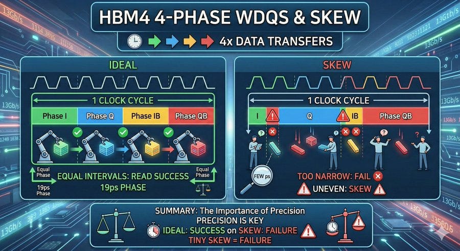
HBM4 uses a quarter-rate 4-Phase WDQS scheme. This means a single clock cycle is divided into four phases — I, IB, Q, QB — enabling four data transfers per clock cycle and effectively quadrupling throughput. But for this to work, the four phases have to be precisely evenly spaced. If the gap between I and IB is narrower than the gap between Q and QB, there isn’t enough time to capture data in the narrow window. This phase imbalance is called skew. At 13Gb/s, each phase window is only about 19ps (picoseconds, or trillionths of a second), so even a few ps of skew is catastrophic.
Traditionally, skew issues were only caught at the SiP (System-in-Package) final test stage — after HBM and GPU have already been assembled into a complete package. Finding a defect there means scrapping the entire assembly, GPU included. On top of that, external test equipment has bandwidth limitations that make it hard to accurately measure high-speed signals, and probing thousands of bumps adds further complexity.
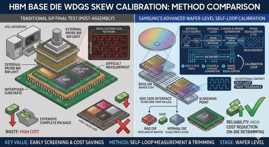
Samsung’s approach is fundamentally different. They use an internal self-loop method that requires no external contact at all. A clock signal generated from a ring oscillator or PLL (Phase-Locked Loop) inside the base die is injected into the WDQS path, flows through the actual WDQS distribution network, and an internal skew monitor measures how far off each phase is. Based on those measurements, skew is automatically corrected per DWORD (32-bit data unit). The correction first aligns the WDQS_T/C (True/Complement differential pair) duty cycle to 50%, then divides the signal by 2 to generate the four phases, and finally equalizes the phase intervals to within a few picoseconds.
The real value here is that the screening point moves to the base die wafer stage. Trim values are determined for each of the 64 DWORDs and recorded via an IEEE 1500 interface. Dies where the trim saturates — meaning the skew is beyond the correctable range — are discarded at the wafer level, before any stacking even begins. That means bad base dies get filtered out before CoW (Chip-on-Wafer) or SiP packaging, avoiding expensive downstream waste. Good dies have their trim values stored and simply loaded during packaging. On-die trimming can also be re-run in the field if operating conditions change.
In actual measured results, applying wafer-level trim to a CoW proxy package running at 10Gb/s reduced RDQS deterministic jitter (DJ) from 10.6ps to 4.5ps — more than halved. DJ measures how far a signal’s timing deviates from ideal, and a lower value means a cleaner, more open data eye, enabling stable high-speed operation.
Key #5: PMBIST — A Testing Revolution Made Possible by Logic Process
HBM is a complex system with thousands of TSVs and dozens of channels, which makes testing it extremely challenging. Fail to catch defective dies early, and you don’t find out until after expensive back-end processes like CoW and SiP packaging have already been completed.

MBIST (Memory Built-In Self-Test) is a self-test circuit embedded directly inside the memory chip — no external equipment needed; the chip tests itself and reports pass or fail. In HBM3E, MBIST was limited to a fixed set of test patterns due to the area constraints of DRAM process technology. Think of it as a multiple-choice exam locked to five fixed questions: any defect that doesn’t happen to trigger those five patterns goes undetected.
HBM4’s PMBIST (Programmable MBIST) is a different beast entirely. Leveraging the area freed up by the 4nm logic process, the test program storage space is roughly 225x larger than before. That fixed five-question multiple-choice test has become a free-form question bank where you can design essays and practical exams. Better yet, test engineers can write test scenarios directly, using an SDK, just like writing code — meaning new defect patterns discovered in the field can be immediately incorporated into future testing. It’s effectively a small dedicated test processor living inside the base die.
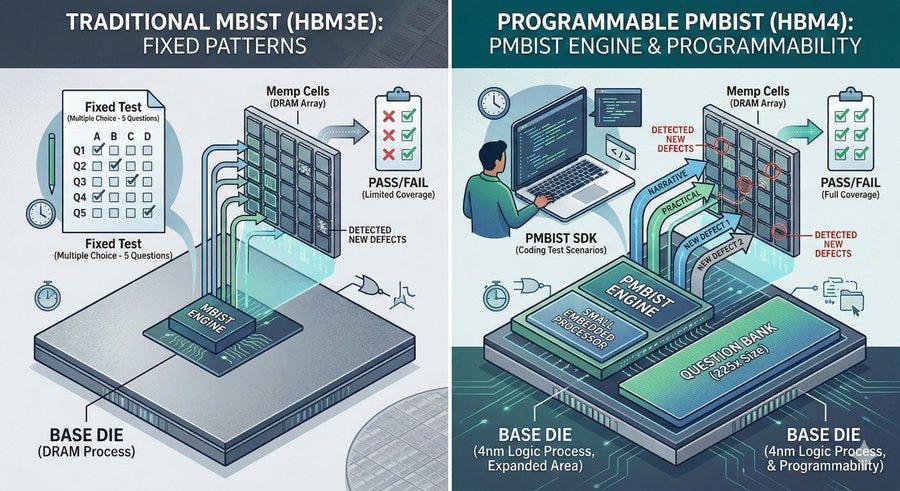
The most meaningful practical difference is flexibility in test ordering. AI workloads have the GPU rapidly switching between dies, and that switching speed (tCCDR) directly affects real-world AI performance. In HBM3E, the fixed test ordering made it structurally impossible to test this switching scenario — there was no way to construct a pattern with rapid cross-die switching. With HBM4 PMBIST, test sequences are freely programmable. You can reproduce an actual AI workload pattern — die 0 → die 1 → die 2, switching rapidly — and test it directly. It’s like an entirely new subject being added to the curriculum.
From a DFT engineer’s perspective, this is a fundamental paradigm shift in test methodology. Defects that previously couldn’t be caught because the test repertoire was too limited can now be systematically targeted with purpose-built scenarios.
Key #6: Bank Architecture Change — Quiet but Meaningful
One more change that tends to get overlooked in generation-to-generation spec comparisons: the bank structure shifted from 4BG × 4BA to 2BG × 8BA.
BG (Bank Group) and BA (Bank) are the organizational units inside memory. Think of memory as a large library: bank groups are the floors, and banks are the reading rooms on each floor. Back-to-back accesses to the same room incur a wait, but switching to a different room allows immediate access. Switching between different floors (bank groups) is even faster.
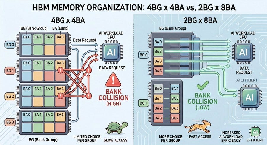
Going from 4BG × 4BA to 2BG × 8BA means the number of bank groups halved (from 4 to 2), but the number of banks within each group doubled (from 4 to 8). The total number of banks (16) is unchanged. The benefit is that within any given bank group, there are now more rooms to pick from. AI workloads tend to involve rapid access across diverse addresses in short time windows, and having more banks per group raises the probability of being able to access sequentially without hitting a bank conflict.
Summary: The Structural Reasons Samsung Could Overtake SK hynix
Stepping back from the technical details, there’s a clear structural logic to Samsung’s HBM4 strategy.
First, this is the first real realization of foundry-memory vertical integration. HBM4 is the first Samsung product to seriously leverage the fact that the company has both foundry (4nm logic) and memory (6th-generation 10nm DRAM) under one roof. The base die logic process transition is a move that would be difficult to execute without that vertical integration — and the advanced capabilities like PMBIST and auto-calibration only become possible because of it.
Second, the aggressive DRAM process generation jump. Skipping 1b and going directly to 1c created the physical preconditions for 2x more DQ TSVs per channel — which, combined with the tighter microbump pitch, enabled HBM4’s expanded channel and I/O configuration. Without this decision, no amount of base die sophistication would have been enough to hit HBM4’s target specs.
Third, fundamental improvements in test and yield. PMBIST (225x more program space, RISC architecture, flexible looping), on-die WDQS skew correction (early screening at wafer level), and tCCDR auto-calibration — together, these create a virtuous cycle of earlier defect detection, higher yields, and optimized real-world system performance. This is Samsung’s structural attempt to reverse the yield advantage SK Hynix built up over HBM3E.
Fourth, a focus on system-level performance. The tCCDR auto-calibration improves not the per-pin speed on a spec sheet, but the performance the GPU actually experiences. Achieving 13Gbps — over 1.6x the JEDEC spec of 8Gbps — while simultaneously optimizing die-switching performance (tCCDR) is a direct shot at NVIDIA’s pain points as a customer.
Open Questions
A single paper doesn’t decide the outcome of a competition. Several critical questions remain.
What is the actual yield of Samsung Foundry’s 4nm process? Is the 1c DRAM process stable in volume production? Can the paper’s performance numbers be reproduced in mass manufacturing? And SK Hynix will almost certainly pursue its own logic base die strategy through its partnership with TSMC — how does that competitive dynamic play out?
But what this paper makes clear is this: Samsung is not simply trying to catch up with HBM4. It’s competing through a differentiated approach built on its own structural strengths. Round two of the HBM race has started.
Appendix: HBM3E vs HBM4 Key Spec Comparison
Process: HBM3E — core and base die both on 4th-gen 10nm DRAM. HBM4 — core die on 6th-gen 10nm DRAM (1c), base die on 4nm FinFET.
JEDEC official data rate: HBM3E 8.0Gbps → HBM4 6.4Gbps
Samsung measured max speed: HBM3E 10.0Gb/s → HBM4 13.0Gb/s.
Channel configuration: HBM3E 16 channels × 2PC × 32 I/O → HBM4 32 channels × 2PC × 32 I/O.
Bank structure: HBM3E 4BG × 4BA → HBM4 2BG × 8BA.
Bandwidth: HBM3E 1.3TB/s per cube → HBM4 3.3TB/s per cube.
Max capacity: HBM3E 24Gb × 16-High = 48GB → HBM4 24Gb × 12-High = 36GB.
Supply voltage (VDDC/VDDQ): HBM3E 1.1V/1.1V → HBM4 1.05V/0.75V.
Microbump pitch: HBM3E 96μm × 110μm → HBM4 70μm × 110μm.
Test approach: HBM3E MBIST (fixed patterns, 2,272 bits) → HBM4 PMBIST (programmable, 512Kbits).
Chip size: HBM3E 11mm × 11mm → HBM4 12.8mm × 11mm.