In AI chips, packaging has become the process that decides performance. As chip miniaturization hits its limits, the method of binding several chips into one has grown more important, and the standard for that is TSMC's CoWoS. TSMC is now preparing CoPoS as the next step beyond CoWoS. Instead of a round wafer, it places chips on a square panel.
Once CoPoS became a talking point, the market went straight to hunting for glass substrate beneficiaries. The reason was the talk that panels use glass. An earlier piece walked through the technology and supply chain of the glass substrate itself, and this time that same glass steps onto the packaging stage, widening the board by one level.

But two things that actually matter are still undecided. First, where exactly glass fits inside the CoPoS structure has not been fixed. TSMC recently showed the possibility by disclosing glass substrate validation results with Ibiden and Innolux, but in the same announcement it drew a line, saying mass production is still far off. Second, this is not a game TSMC decides alone. Intel and Samsung are each pushing panel packaging and glass in their own way, so even which camp and which method wins is still open.
To put it together, the direction of CoPoS is clear but the path and the timeline are both uncertain. In a situation like this, picking stocks off the single word “glass” leaves you most exposed when glass lands in a different spot than expected, or when mass production slips.
So the question to throw out is a different one.
Whatever form glass comes in, and whether mass production is fast or slow, which seat survives? Lay the CoPoS beneficiaries across two coordinate axes and that seat comes into view.
Contents
The terrain: what CoPoS changes and what it does not
The map’s two axes: purity and path survival
The stock map by coordinate
How to read and track the map
The risks that shake the map
Disclaimer
This piece is written for the purpose of information and industry analysis, and does not recommend buying or selling any security. The companies and stocks that appear in the body are objects of analysis used to explain the CoPoS supply chain, not recommended investments. The coordinate classifications, portfolio role divisions, and scenarios in the body are the author’s personal analytical framework, not advice tailored to any individual’s investment situation. The author is not a registered investment adviser, and this piece does not constitute quasi-investment advisory or investment solicitation. The author may hold or later trade the stocks mentioned, and that fact is not grounds for any recommendation. All investment decisions and their consequences rest entirely with the investor. The figures and timelines in the body are based on public materials and company announcements as of the time of writing, and may differ from fact or change with market conditions.
1. The terrain: what CoPoS changes and what it does not
Before drawing the map, look at the terrain. CoWoS stands for Chip on Wafer on Substrate. The chip sits on an interposer made from a round silicon wafer (an interposer is the middle layer that runs fine wiring between chip and substrate), and that is attached to a substrate. CoPoS is Chip on Panel on Substrate. The middle word changed from Wafer to Panel. Instead of a round wafer, it uses a square panel.
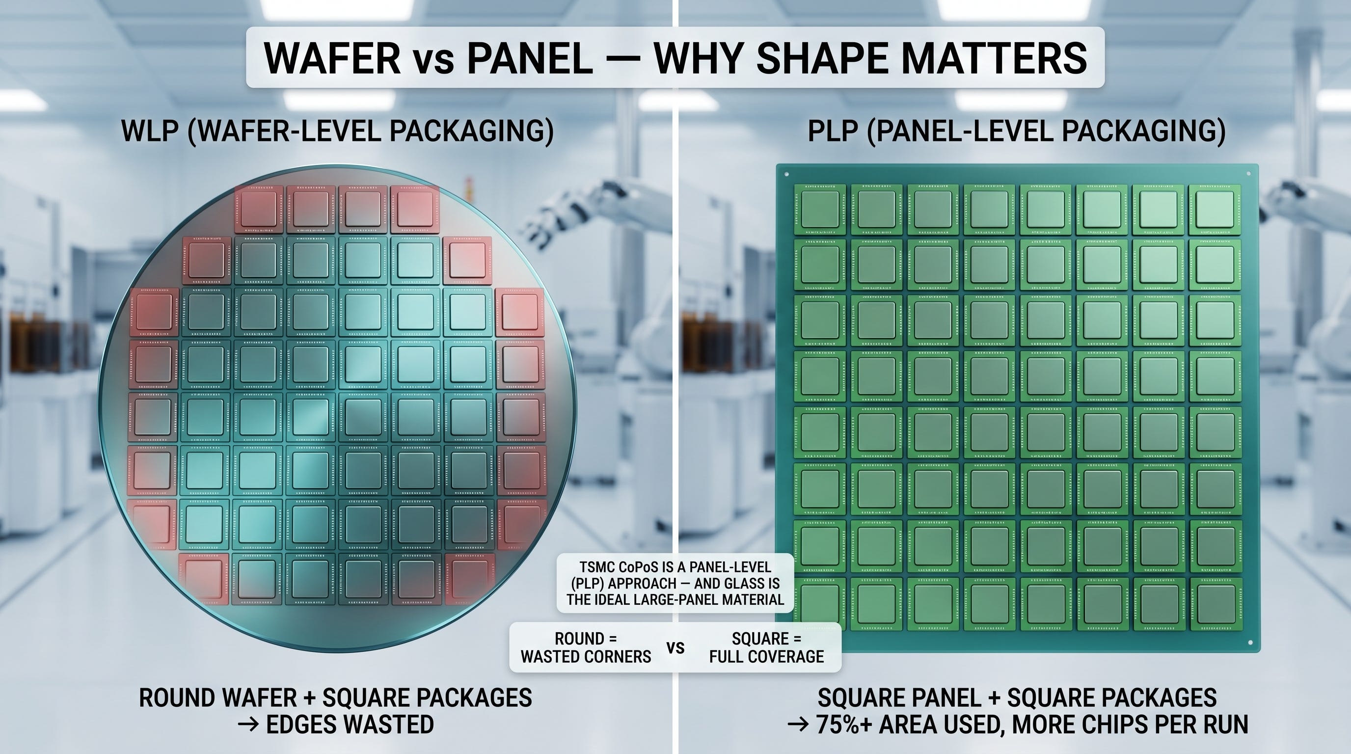
Why square? Area. The chips in AI accelerators keep getting bigger. They are expressed as multiples of the reticle, the unit a single exposure shot covers. Place a package this large on a round 12-inch wafer and the edges go to waste, yielding only four to seven per sheet. A square panel loses less at the edges and pulls far more from the same area. TSMC’s first panel format is 310mm by 310mm, and a roadmap is cited that grows it through 515mm by 510mm up to 750mm by 620mm.
The timeline runs like this.
The pilot line gets laid down at the subsidiary VisEra in 2026. VisEra is a TSMC subsidiary with panel-processing experience built from wafer-level optical work for image sensors, and it takes the pilot role of validating the CoPoS process ahead of the mass-production sites. By press accounts, small trial production is cited for 2027 and mass production for 2028 to 2029.
That said, reading TSMC’s own comments alongside supply-chain commentary, the weight falls on the view that meaningful mass production needs another two to three years of validation. The mass-production site is the fourth phase of the AP7 campus in Chiayi, Taiwan, and the first customer is cited as NVIDIA.
Look at the roadmap alone and the picture seems clean. But from an investment standpoint, two things that have not yet set are hiding inside this roadmap, and those two are exactly where the map begins.
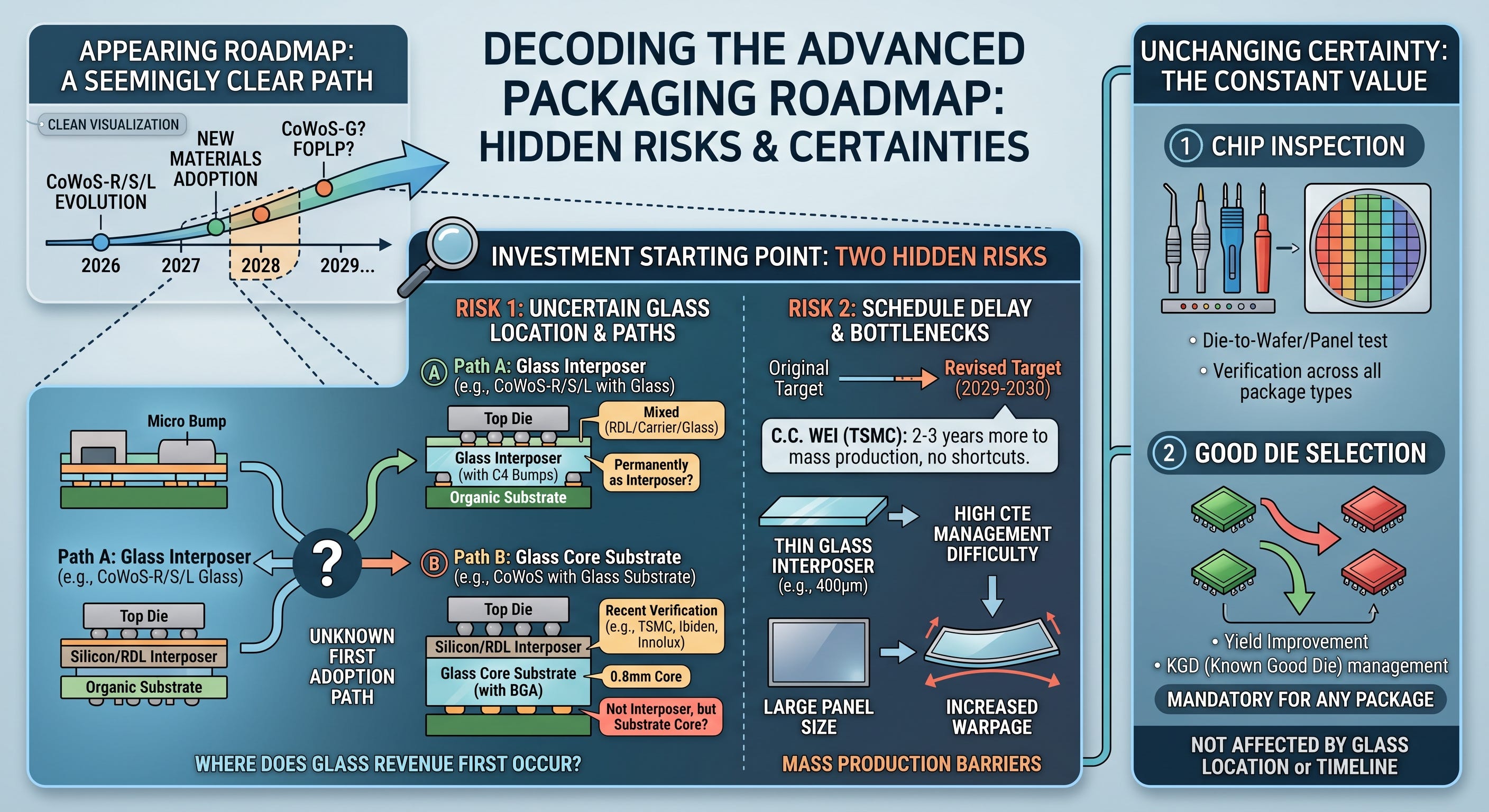
First, glass’s position is not yet fixed.
Many explanations say CoPoS uses glass as the interposer, but the wording splits by source. Some see CoPoS as a transition that mixes panelization, redistribution layer (RDL), carrier, and glass or organic material, while others flatly call glass a permanent interposer.
The recent validation mentioned above only deepens this uncertainty. What TSMC validated with Ibiden and Innolux was not an interposer but a 0.8-millimeter glass core substrate, and the program was even named “glass substrate for CoWoS.”
It means it has not yet set in one direction whether glass comes in as an interposer or as a core substrate, and which path reaches mass production first. So what to watch is not the fact that glass goes in, but which bottleneck in the panel process turns into revenue first.
Second, the weight is on the timeline slipping.
TSMC Chairman C.C. Wei nailed it down: mass production takes another two to three years and there are no shortcuts.
When glass is used as a thin interposer, its thickness drops to about 400 micrometers, half that of a substrate, making CTE (coefficient of thermal expansion) management tricky, and whatever form it takes, warpage worsens as the panel grows. This physical constraint is repeatedly cited as the biggest barrier to mass production. On the ground, some see mass production landing in 2029 to 2030.
Meanwhile, this transition has an unshakable part too.
However chip and substrate are bound, they must pass inspection, and screening out good dies in advance is a step no package skips. Whatever glass comes in as, and whether mass production is fast or slow, this area does not change.
So when choosing CoPoS stocks, the question to throw out gets simple. With both glass’s position and the mass-production timeline uncertain, which stock gets hit hard when this transition succeeds, and which one holds even when the transition slips or goes sideways? Split this question into two axes and it becomes a map that lines the stocks up.
2. The map’s two axes: purity and path survival
The question above forks two ways. One is “if this transition succeeds, how much does the stock get hit,” and the other is “even if the transition slips or goes sideways, does the stock hold.” Put the first on the horizontal axis and the second on the vertical.
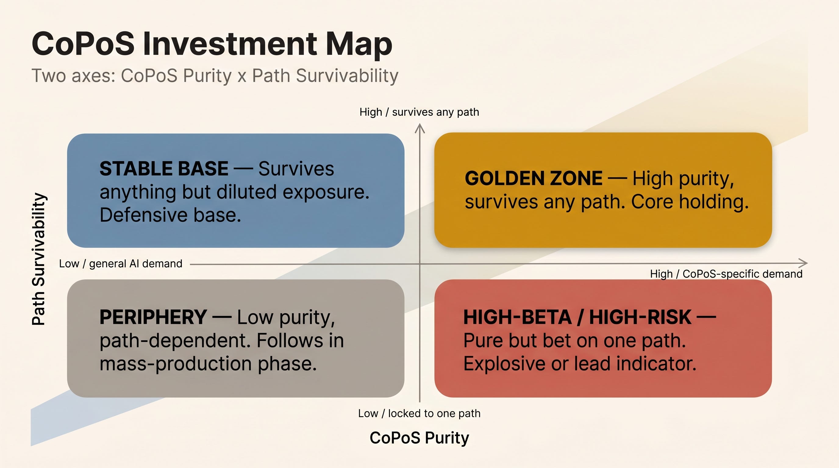
The horizontal axis is CoPoS purity.
It divides whether the company’s demand comes directly from the CoPoS transition, or whether it rides along because AI overall is growing.
Demand that did not exist in the silicon interposer era, like glass carriers and through-glass via (TGV) equipment, has high purity. Demand that grows because of AI heat or memory stack count occurs whether the format is panel or wafer, so its purity is low. The higher the purity, the bigger the explosive payoff when CoPoS succeeds.
This is the answer to the first question, “how much does it get hit if it succeeds.”
The vertical axis is path survival.
CoPoS is not the only future of AI packaging. The NVIDIA Rubin Ultra generation goes with a mix of CoWoS and CoPoS, and beyond that even CoWoP (Chip on Wafer on PCB), which drops the substrate and attaches the chip directly to the PCB, gets cited. That is at least three paths.
Items used only on panel glass, like glass carriers and TGV equipment, have their revenue tied to the single CoPoS path. Inspection and metrology are needed on any path, whether CoWoS, CoPoS, or CoWoP. The higher the path survival, the less value gets cut when the timeline slips or the path splits.
This is the answer to the second question, “does it hold if things go sideways.”
Overlay the two axes and the uncertainty from the previous chapter unfolds right onto the coordinates. That glass’s position is undecided means a stock can shake even at high purity if the path splits, and that the timeline is undecided means the lower a stock sits on the vertical axis, the more dangerous it is.
And the fact that inspection is needed regardless of path means inspection stands at the very top of the vertical axis.
There is one more reason for placing inspection at the top of the vertical axis. The glass transition is likely to create demand closer to equipment replacement than to a simple capacity addition.
The mainstay of package inspection so far, automated optical inspection (AOI), fires light and reads surface reflection. But glass runs into bigger limits with conventional surface AOI because of transparency, reflection, internal defects, and TGV cracks, so demand grows for more complex inspection like infrared (IR) transmission inspection, 3D metrology, X-ray, and high-sensitivity optical inspection. So glass inspection is closer to switching over to a new kind of equipment than to adding incremental units of the old.
Especially in the early mass-production phase, near-total in-line inspection demand can grow to stabilize yield, and the equipment to run that inspection has to be brought into every line anew. It means that before the mass-production volume ramps, inspection equipment goes in first, from the validation and qual stages. That is why, among the same CoPoS beneficiaries, inspection is the one most likely to turn into revenue first.
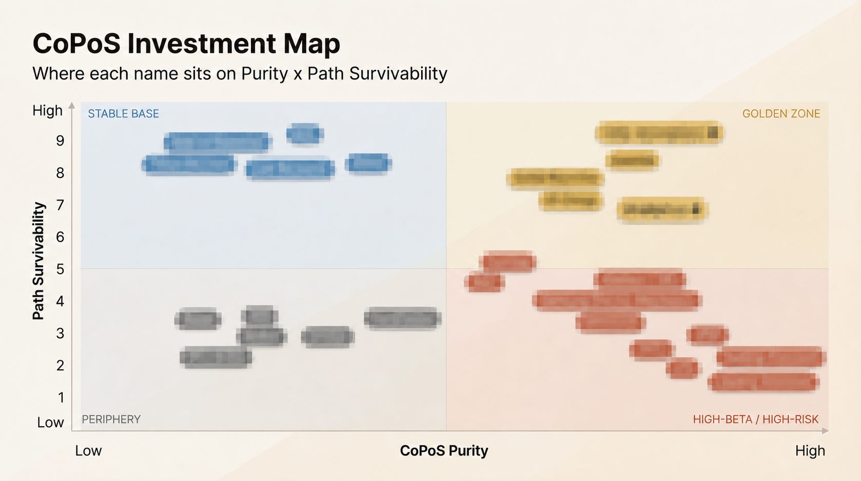
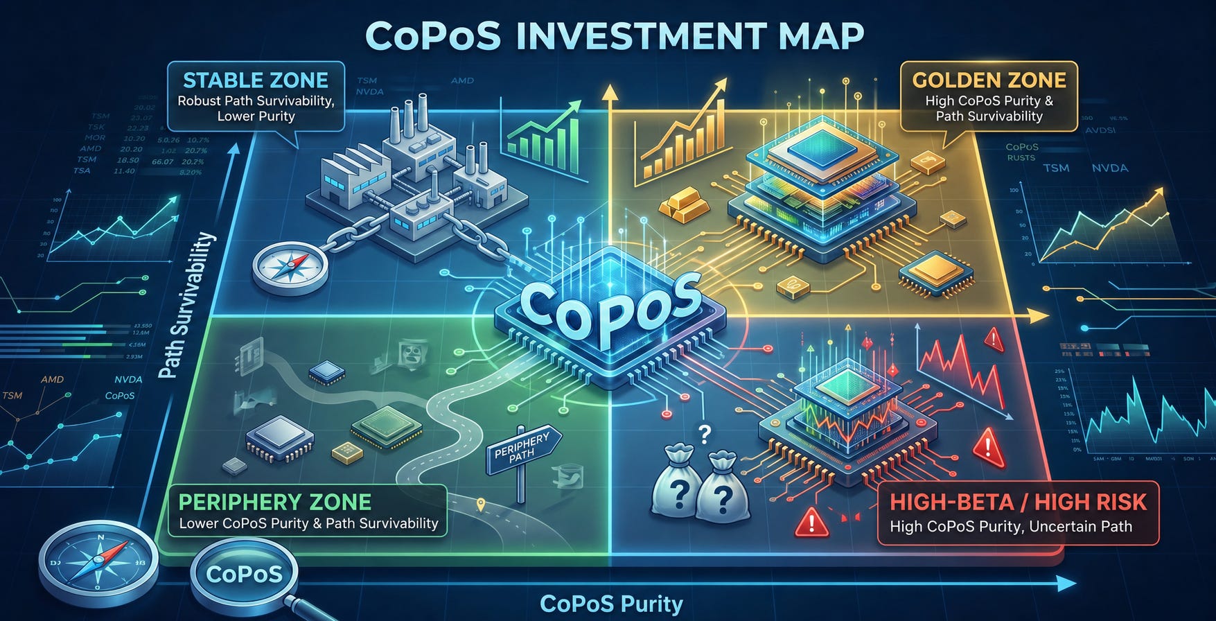
The four quadrants these two axes make decide the investment meaning. The further right on the horizontal axis, the higher the CoPoS purity, and the higher on the vertical axis, the higher the path survival. The upper right is the golden coordinate that holds both purity and survival, the lower right is the high-explosive coordinate that has high purity but is tied to one path, the upper left is the stable core whose survival is high but whose exposure is thin, and the lower left is the peripheral area that tags along in the mass-production phase.
The real difference is between the upper-right golden coordinate and the lower-right high-risk coordinate. Both have high CoPoS purity. But the golden coordinate lives even when the path splits, while the high-explosive coordinate is tied to the single CoPoS path. On the premise that the timeline slips, this difference on the vertical axis decides the match.
That covers the two axes that frame the map. With the axes drawn, the real question remains: where do the names currently lumped together and traded as "glass plays" actually land on this map? The moment you place each stock at its own coordinate, what to buy and what to avoid comes into focus.