


Introduction
As we enter the AI era, the importance of memory, led by HBM (High Bandwidth Memory), has never been greater. AI semiconductors from NVIDIA, AMD, and others cannot achieve their full performance without HBM. So how exactly do we test this memory?
My doctoral research lab focused on Design for Test (DFT) for semiconductor testing and was one of the world’s most renowned research groups in memory testing and repair. Today, I’ll explain the fundamentals of memory testing methodology from my doctoral research and industry experience in a way that even non-specialists can understand.
Substack is currently in a trial phase, so all premium quality articles are available for free for now. Once paid subscriptions are introduced, pricing will be set at a level comparable to professional tech writers on Substack. Early supporters will have the benefit of locking in their current pledge price for future paid access.
1. What is Memory Testing?
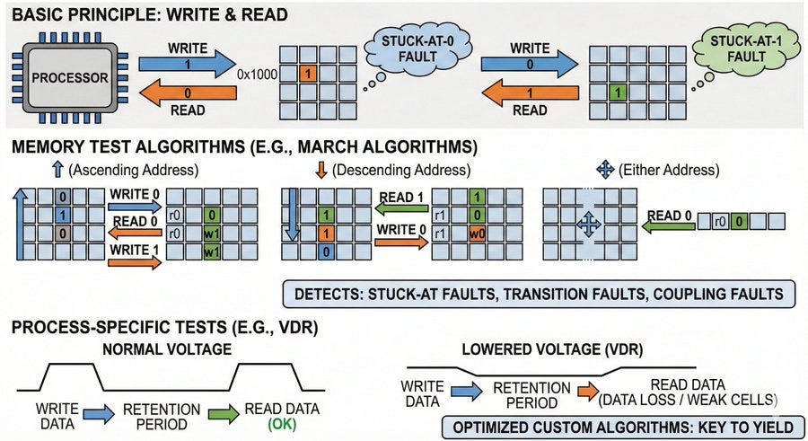
Basic Principle: Write and Read
The most fundamental principle of memory testing is simple. Write a value to a specific address, read it back, and verify that the read value matches what was written. If the written and read values differ, the bit cell is determined to have a fault.
For example, if you write ‘1’ to address 0x1000 and read back ‘0’, that cell has a Stuck-at-0 fault. Conversely, if you write ‘0’ but read ‘1’, it’s a Stuck-at-1 fault.
Memory Test Algorithms
However, simply writing 0s and 1s to all cells and reading them back cannot detect all faults. Systematic algorithms are needed to detect interactions between memory cells, known as Coupling Faults.
March algorithms are the representative family of memory test algorithms. Various variants exist such as March C-, March LR, and March SS, each capable of detecting different fault types. The basic structure of March algorithms is as follows:
⇑ (Ascending): Perform operations while incrementing addresses from 0 to the end
⇓ (Descending): Perform operations while decrementing addresses from end to 0
⇕ (Either): Perform operations in either direction
For example, the March C- algorithm consists of 6 elements: {⇕(w0); ⇑(r0,w1); ⇑(r1,w0); ⇓(r0,w1); ⇓(r1,w0); ⇕(r0)}, capable of detecting Stuck-at Faults, Transition Faults, and some Coupling Faults.
Process-Specific Test Algorithm Implementation
Beyond standard March algorithms, specialized tests exist that consider memory characteristics. A representative example is VDR (Voltage Drop Retention) testing. This method tests retention characteristics while intentionally lowering the operating voltage, filtering out weak cells with insufficient voltage margins. Marginal defects that pass at normal voltage but fail at lower voltage are often the culprits behind intermittent field failures.
In actual production environments, defects often concentrate at specific locations or conditions depending on process characteristics, leading to the development of process-tailored test patterns. Ultimately, how deeply each company understands its process’s defect characteristics and possesses optimized custom algorithms determines its yield competitiveness.
2. Why is MBIST Necessary?
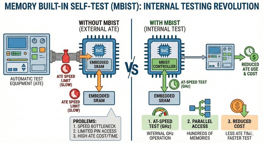
Memory Built-In Self-Test (MBIST) embeds memory test circuitry inside the chip, enabling self-testing of memory with minimal ATE usage. So why do we design MBIST instead of directly testing memory with ATE?
First, speed. When testing memory through ATE, the interface speed between the ATE and chip becomes a bottleneck. Modern SoC embedded SRAM operates at GHz speeds, which external testers cannot match. MBIST enables At-Speed testing inside the chip.
Second, accessibility. Modern SoCs contain hundreds of memory blocks. Directly accessing all these memories through external pins is physically impossible. MBIST can access all memories through internal test structures such as IJTAG or IEEE 1500.
Third, cost. Reducing usage time of expensive ATE equipment lowers test costs. MBIST can test multiple memories simultaneously in parallel, also shortening test time.
3. What is Memory Repair?
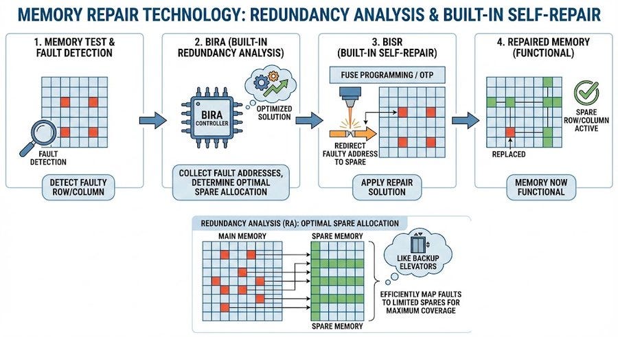
Unlike logic, memory can improve yield through repair. Memory repair is a technology that replaces defective rows or columns with spare rows/columns. It’s similar to installing backup elevators in a building and switching to backup when the main elevator breaks down.
Redundancy Analysis (RA)
RA is the algorithm that determines which spare row/column should replace which defective row/column. Rather than simply replacing with spares whenever a defect is found, optimization is needed to cover as many defects as possible with limited spare resources. For example, if multiple defects exist in the same column, column repair may be more efficient than row repair.
BIRA and BISR
BIRA (Built-In Redundancy Analysis) is an on-chip algorithm that analyzes defect information to find optimal repair solutions. It collects defect addresses found during testing and determines spare row/column allocation.
BISR (Built-In Self-Repair) is the stage that actually applies the repair information determined by BIRA. Typically, fuses are programmed so that accessing a defective address automatically redirects to spare rows/columns. Recently, eFuse or OTP (One-Time Programmable) memory is also used.
4. Difference Between ECC and Memory Repair
ECC (Error Correction Code) and memory repair both address memory defects, but differ in application timing and purpose.
Memory repair physically replaces defects occurring during manufacturing. Once repaired, it operates like a normal cell with no runtime overhead.
ECC detects and corrects transient errors (Soft Errors) occurring at runtime. It addresses temporary phenomena like bit flips caused by cosmic rays or alpha particles. SECDED (Single Error Correction, Double Error Detection) is representative, correcting 1-bit errors and detecting 2-bit errors.
In practice, HBM and GDDR6 use both technologies together. Repair removes Hard Faults during manufacturing, while ECC handles Soft Errors during operation. From HBM3 onward, On-Die ECC became a mandatory specification to address additional defects that can occur in stacked structures.
5. Actual Test Flow: From GO/NO-GO to Bitmap
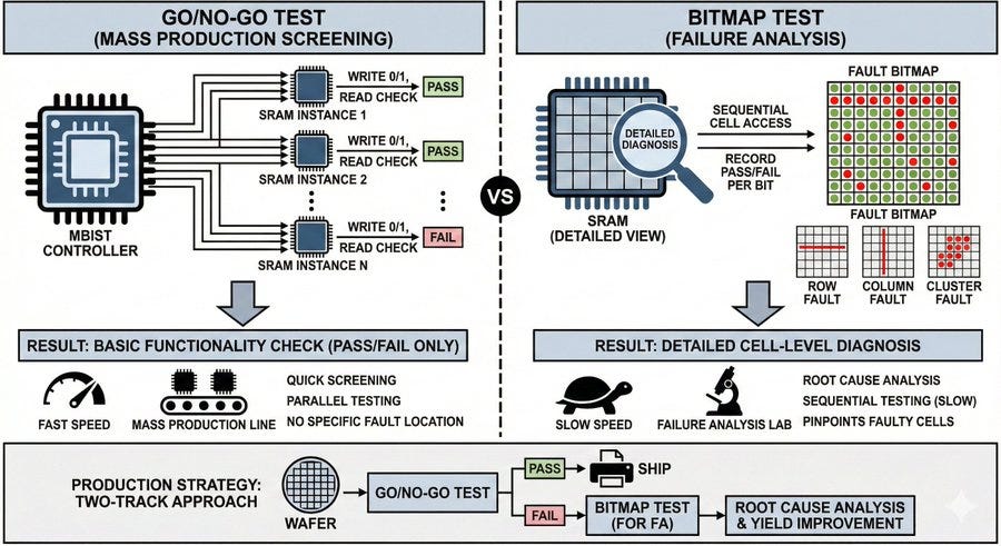
In actual production environments, memory testing proceeds in stages. Multiple memory blocks are tested simultaneously in parallel through MBIST, with test depth varying by purpose.
GO/NO-GO Testing
The first stage is GO/NO-GO testing. It quickly determines whether memory is basically functional, simply whether it’s alive or dead. Writing 0s and 1s to all bits and reading them confirms only Pass/Fail. This stage can determine whether memory defects occur in the chip, but cannot identify exactly which memory or which memory cell is defective.
Bitmap Testing and Its Limitations
When GO/NO-GO fails, Bitmap testing is performed to precisely identify which bit cells are defective. It records Pass/Fail information individually for every bit position.
Bitmap testing is a powerful diagnostic tool but has a critical drawback. Since defective cell information for each memory must be stored sequentially, parallel testing is impossible, and test time increases exponentially for large-capacity memory. Therefore, it’s used only for Failure Analysis (FA), not production lines.
Bitmap results play a key role in identifying defect causes. If defects concentrate in specific rows or columns, Row/Column Decoder problems can be suspected. If they appear in cluster patterns, process particle contamination is likely. Based on such analysis results, new test algorithms may be developed for yield ramp-up stages. Ultimately, production uses a two-track strategy: quick screening with GO/NO-GO, with separate Bitmap analysis only for problematic chips.
Why Memory Testing Follows Logic Testing
Memory testing is generally performed after logic testing (Scan Test). This isn’t simply a matter of sequence but has technical and strategic reasons.
First, the MBIST controller is part of the logic. Testing memory requires the MBIST controller to function properly, but this controller itself is logic circuitry. If the logic has faults, MBIST won’t operate correctly, making memory test results unreliable.
Second, clarity in test result interpretation. If memory testing fails without knowing whether logic is normal, it’s impossible to distinguish between actual memory defects and MBIST controller faults. Logic must first be confirmed normal through Scan Test before memory test results can be trusted.
Third, yield strategy. Memory can be repaired through spare rows/columns, but logic faults cannot be repaired. Therefore, from a yield improvement perspective, it’s more efficient to first secure unrepairable logic yield, then proceed with memory testing and repair.
6. HBM Testing: Challenges of 3D Memory Structure
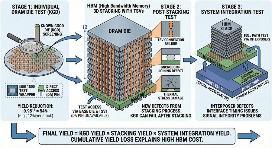
HBM is a 3D structure where multiple DRAM dies are vertically stacked and connected via TSV (Through-Silicon Via). This structure is the fundamental reason why improving HBM yield is difficult. Unlike conventional single-die memory, yield multiplies at each stage.
Stage 1: Individual DRAM Die Testing (Known Good Die)
Before stacking, each DRAM die is individually tested to select Known Good Die (KGD). For example, with 12-layer stacked HBM3E, even if individual die yield is 95%, simple calculation gives 0.95 to the 12th power, approximately 54%. If even one defective die is included, the entire HBM becomes defective, so KGD selection accuracy determines final yield.
Two test access approaches exist. The HBM JEDEC specification adopts IEEE 1500 standard-based test wrappers, enabling standardized test access. Additionally, before stacking, each die’s memory can be directly accessed and tested through DA (Direct Access) pins.
Stage 2: Post-Stacking Testing
Once dies are stacked, DA pins on memory dies can no longer be used. Testing is now only possible through the Base Die, with test structures implemented in the Base Die accessing upper dies’ memory through TSV.
The problem is that the stacking process itself creates new defects. TSV connection defects, micro bump bonding defects, and defects from thermal stress during bonding can occur. Even dies selected as KGD can become defective after stacking, making retesting essential. Considering stacking process yield, final yield drops further.
Stage 3: Post-System Integration Testing
After HBM is connected to host chips like GPUs or AI accelerators through interposers, final memory testing is performed at the system level. The entire memory path including interposer connections is tested through the host chip’s memory controller.
Yield loss occurs again at this stage. Interposer bonding defects, HBM-host interface timing issues, and signal integrity problems may be newly detected. Ultimately, final yield equals KGD yield × stacking process yield × system integration yield. This is the structural reason why HBM prices are high.
Conclusion
Memory testing and repair technologies are core technologies determining semiconductor yield. On top of the seemingly simple principle of “write and read,” various technologies are layered: March algorithms, MBIST, BIRA/BISR, and ECC.
As we enter the HBM era, test complexity continues to increase. 3D stacked structures create new defect possibilities at each stage, and test strategies must evolve accordingly. The importance of KGD selection, necessity of post-stacking retesting, and multi-stage test systems extending to system-level integration testing guarantee HBM quality.
As the AI semiconductor market grows, the role of memory test engineers becomes increasingly important. Faster, more accurate, and more efficient test technologies will enable the next generation of AI accelerators.