

Intel is back at the center of the market.
On April 24, Intel’s stock surged 24% in a single day. It was the largest one-day gain since 1987. For the month of April, shares rose 114%, one of the strongest monthly rallies in Intel’s history, touching $100 intraday. That’s a price level not seen since the dotcom bubble of 2000.
The surface-level trigger was Q1 earnings. Revenue came in at $13.6B, with non-GAAP EPS of $0.29, blowing past the Street consensus of $0.01. Data center and AI revenue hit $5.1B, up 22% year over year. Q2 revenue guidance of $13.8B to $14.8B also topped the $13.07B consensus.
But a move of this magnitude is hard to explain with one quarter of results. The good numbers were just the trigger. What the market started re-evaluating wasn’t Intel’s earnings per se, but the structural shift behind them.
So what exactly is the market starting to see differently?
I previously wrote an article titled “Intel Foundry: The Last Chance.” As a former foundry engineer, I covered the technical challenges Intel Foundry needed to overcome, drawing on my own foundry knowledge and looking from the outside in.
Intel Foundry: A Last Chance

In Q4 2025, Intel Foundry posted revenue of $4.5 billion alongside an operating loss of $2.5 billion. CEO Lip-Bu Tan admitted that “the company invested too much, too fast, without sufficient demand,” and Intel’s SEC filing included risk language to the effect that the company has yet to secure meaningful external foundry customers at scale on any of it…
But I felt my knowledge alone wasn’t enough to explain what’s changing at Intel right now. So I met with and interviewed someone currently working on Intel’s foundry research team. It gave me a direct look at Intel’s technology strategy and internal engineering perspective that public materials alone don’t capture.
Intel’s strength isn’t about having one good process node or one good package. It’s about the ability to translate a customer’s software-level requirements into actual technology knobs, and to bind transistors, circuits, packages, power delivery, memory, optics, and system architecture into a single optimization loop.
That structure has a name, STCO, System Technology Co-Optimization.
The central question of this article is straightforward. Is Intel just an old CPU company enjoying a temporary bounce? Or is the market beginning to re-rate it as a full-stack semiconductor company that AI actually needs?
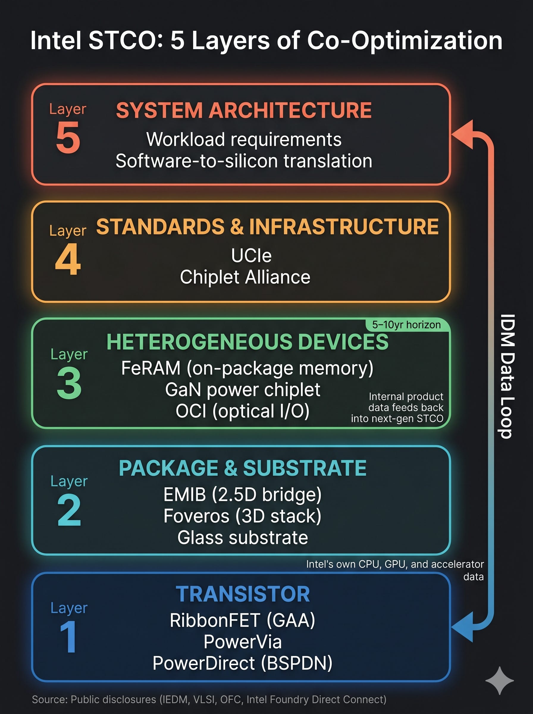
The answer becomes visible when you unpack Intel's STCO assets layer by layer. This article first defines what STCO is, then walks through five layers of technical assets: transistors, packaging, heterogeneous devices, standards and infrastructure, and system architecture. From there, it examines four paths along which Intel's profitability is actually improving, identifies signals that strengthen or weaken the thesis, and finally lays out the value chain beneficiary map that STCO opens up.
Disclaimer
This article is written for informational and analytical purposes and does not constitute investment advice recommending the purchase or sale of any specific security. Earnings figures, company announcements, and technical specifications cited here are based on publicly available information at the time of writing and may change. All investment decisions and their outcomes are solely the responsibility of the reader. The author assumes no liability for any investment losses.
1. What STCO Is and Why It’s Intel’s Moat
STCO didn’t appear out of thin air. It’s easier to understand if you start with DTCO.
DTCO stands for Design Technology Co-Optimization.
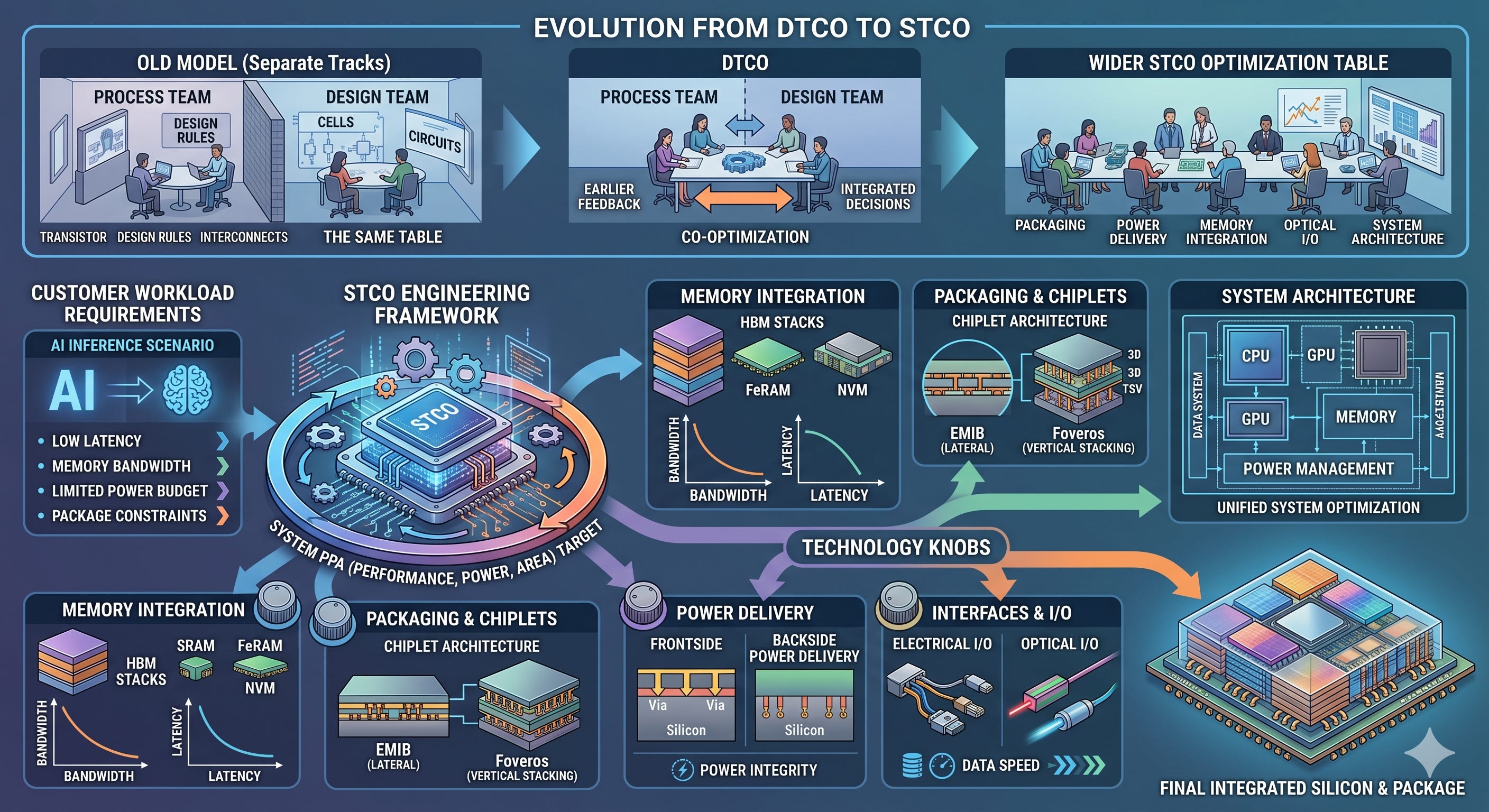
Instead of treating process and design as separate tracks, you optimize them together. In the old model, the process team would define transistor characteristics, design rules, and interconnect specs. Then the design team would draw cells and circuits within those constraints. But as nodes shrank, this approach hit limits. Making transistors slightly smaller wasn’t enough anymore. Teams needed to see earlier how process choices affected real circuit performance, power, and area. So the process team and the design team started sitting at the same table. That’s DTCO.
STCO widens that table.
Now the optimization scope doesn’t stop at transistors and circuits. It extends to packaging, power delivery, memory integration, optical interfaces, and system architecture. The problem isn’t just how to make a good chip. It’s how to architect the entire system the chip goes into.
Inside Intel, STCO is less a marketing term and more an engineering framework. It starts with the customer’s software-level requirements for performance, power, bandwidth, and latency, then translates those into specific process choices, package structures, power delivery schemes, and interface specs. Put simply, it’s the work of converting a customer’s workload requirements into actual silicon and package technology knobs.
Here’s what that looks like concretely. Say a customer wants to reduce latency on an AI inference workload. Memory bandwidth is tight, the power budget is limited, and the package can’t grow indefinitely. STCO takes those requirements and translates them into a set of simultaneous questions. Which transistor library? How many chiplets? How much SRAM, and should FeRAM or other memory blocks be in the mix? How many HBM stacks, and where? Attach them laterally with EMIB, or stack vertically with Foveros? Is frontside power delivery enough, or is backside power needed? Is electrical I/O sufficient, or does this need optical I/O? And how do all of these choices affect system-level PPA?
STCO is the process of coordinating these questions under a single system PPA target, rather than having each team solve them independently. The technical assets are the raw materials. STCO is the methodology for combining them. That’s why this article unpacks the technology layer by layer. Each layer is a knob that STCO turns, and whether those knobs can move together inside the same loop is the core of the Intel thesis.
2. The Transistor Layer: RibbonFET and PowerVia
At the very bottom of STCO sits the transistor. Every system optimization ultimately starts with how well you control current and how efficiently you deliver power.
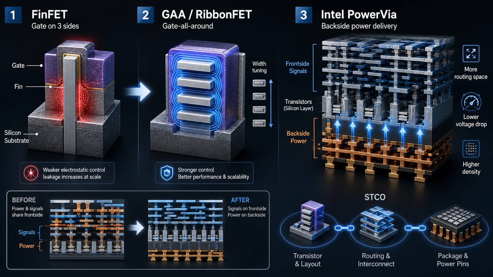
For the past decade, the industry’s workhorse transistor structure has been FinFET. As the name suggests, FinFET uses thin, fin-shaped channels that the gate wraps around on three sides. The industry rode this structure from the 16nm and 14nm generation through 5nm. But as nodes shrank, the gate’s ability to control the channel started weakening. Leakage current became harder to contain, and balancing performance against power grew increasingly difficult.
That’s why the industry is transitioning to the next-generation structure: GAA, Gate-All-Around. As the name implies, the gate wraps the channel on all sides. Where FinFET covered three faces, GAA covers top, bottom, and both sides. It enables more precise current control and finer tuning of performance and power characteristics by adjusting channel width.
Intel calls its GAA implementation RibbonFET. TSMC introduces GAA starting with N2, and Samsung adopted it earlier at 3nm, though production stabilization took time. Up to this point, the entire industry is heading in the same direction. Intel’s unique story starts with what comes next.
That card is PowerVia.
Look at a cross-section of a conventional chip. Transistors sit at the bottom, with multiple metal layers stacked above. These metal layers carry two things simultaneously: data signals and power. The problem is that as nodes shrink, wiring space gets tighter. Signal lines and power lines share the same real estate, and they start interfering with each other. Thicker power lines crowd out signal routing. More signal lines compromise power delivery.
PowerVia changes this structure. Data signals still go out through the front side of the chip. But power is delivered from the back side. After fabricating the wafer, the backside is processed to lay down dedicated power delivery metal, feeding power directly to transistors from below. The industry term for this is BSPDN, Backside Power Delivery Network.
The benefits are fairly intuitive. Removing power lines from the front-side metal layers frees up space for signal routing. Routing becomes easier, and the same functionality fits into a smaller area. Power also reaches transistors through a shorter path, reducing voltage drop (IR drop). Lower voltage drop means more stable performance at the same power budget, and it’s easier to pack more transistors into the same area.
Intel’s published numbers show cell utilization exceeding 90% with PowerVia, a 5% to 10% improvement over baseline. Performance gain at iso-power is up to 4%. Looking at the full 18A node, Intel claims 15% better performance per watt and 30% higher density compared to Intel 3.
The important thing here isn’t the 4% number itself. PowerVia is not a technology the process team can deliver alone. To feed power from the backside, the transistor layout, frontside signal routing, backside power routing, and package power pin placement all have to align. An optimization on one side can create a conflict on the other. For example, the locations where backside vias need to be drilled might overlap with where the frontside signal routes want to go. Or the package power feed points might not match the chiplet floorplan.
This is why PowerVia isn’t just a process technology. It’s an STCO-level technology. For foundry customers, the implications shift too. It’s no longer just about whether this node is a few percent faster than TSMC. It’s about whether you can co-optimize power delivery architecture, package pin maps, and chiplet floorplans together. For AI chips where power and routing are simultaneous bottlenecks, this difference can be significant.
That said, the decision to introduce both RibbonFET and PowerVia simultaneously at 18A was not the easy path. Layering a new transistor architecture with a new power delivery architecture in the same node multiplies the variables to debug. When something goes wrong, isolating whether the root cause is the transistor structure, the backside power delivery, routing, or package interaction becomes harder. Introducing them one generation at a time might have made yield ramp smoother.
The fact that 18A goes into Intel’s own Panther Lake product before external customers also makes sense in this context. Intel can run a full silicon cycle on its own product first, stabilizing the process-design-package interactions. The data generated in this process feeds into future foundry customer support. The IDM data loop mentioned earlier shows up here again.
TSMC is heading in the same direction. TSMC calls its backside power structure Super Power Rail and plans to pair it with nanosheet transistors at the A16 generation. Intel’s advantage isn’t a permanent moat. It’s closer to a time gap before TSMC catches up. But TSMC’s customer base and execution track record are formidable. So how long this time gap lasts depends on how many external customers Intel can win and how much it can prove with real products in the interim.
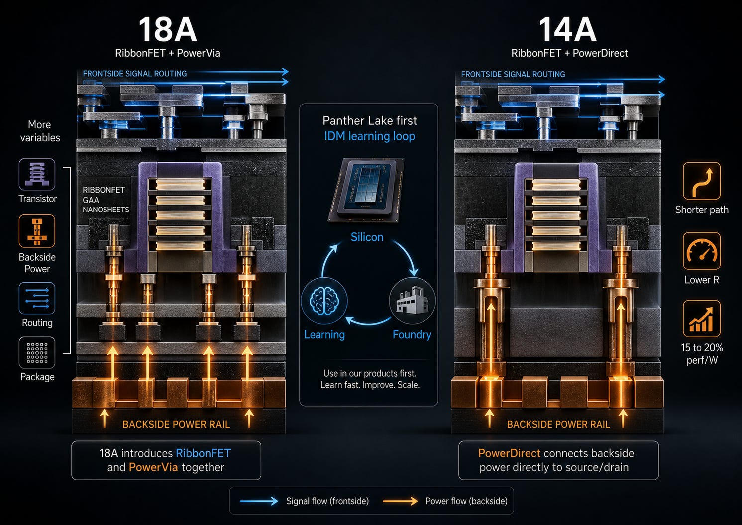
At 14A, things go a step further. If PowerVia delivers power from the chip’s backside, PowerDirect connects backside contacts more directly to the transistor’s source and drain. Fewer intermediate steps mean lower resistance, yielding additional efficiency and area benefits. Intel has indicated that the RibbonFET plus PowerDirect combination could deliver 15% to 20% improvement in performance per watt.
The node Tesla mentioned in its Terafab concept is this same 14A. Ultimately, 14A isn’t just the next process node. It’s the stage where Intel has to prove RibbonFET, backside power, advanced packaging, and the external foundry model all at once. PowerVia and PowerDirect are the transistor-layer cards that underpin the entire thesis from the bottom up.