The re-rating of the AI semiconductor value chain has happened in the order of visibility. First it was GPUs. Then foundries. Then memory. Stock prices moved in the order the market recognized each bottleneck.
So where is the next re-rating?
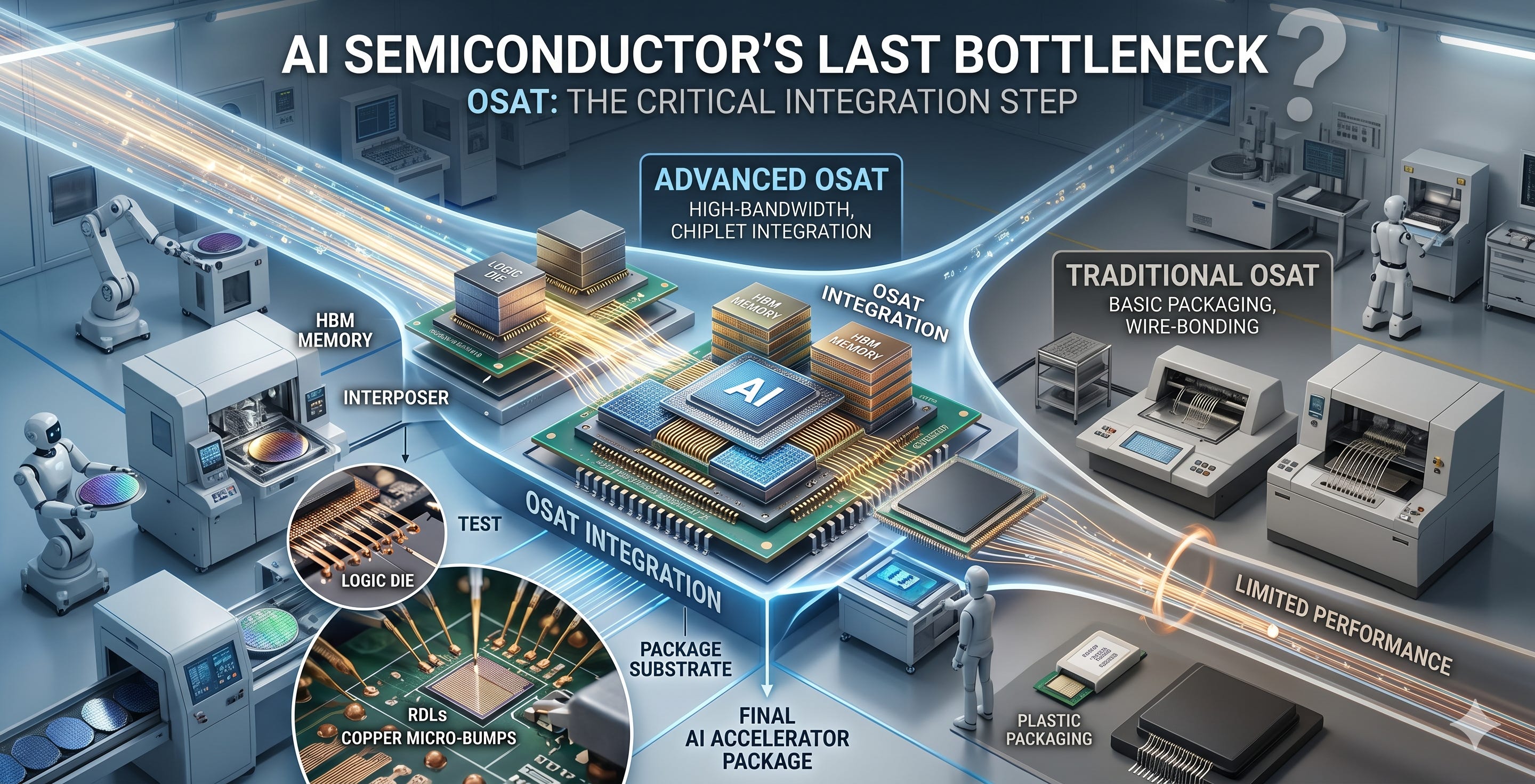
There is one final stage in semiconductors that the market doesn’t know well. Even after design, fabrication, and memory attachment, a chip is still not finished. It has to be diced, stacked, connected, and tested through backend processing before it becomes a chip. The companies that handle this segment are OSATs (Outsourced Semiconductor Assembly and Test).
For a long time, the market looked at OSAT through a narrow lens. Backend outsourcers. A commodity where it doesn’t matter who does the work. But as the AI era arrived, that label stopped fitting. Even within OSAT, some revenue generates 10% margins while other revenue produces EBITDA margins above 40%. I believe this segment is the last part of the AI semiconductor value chain that will re-rate.
In this article, I decompose the revenue of 12 publicly listed OSATs to analyze how the profit structures of low-margin assembly and high-margin test differ, whether the market has priced in this difference, and which OSATs retain investment value along the time axis.
Disclaimer: This article does not constitute a recommendation to buy or sell any specific security. All investment decisions and their consequences are the sole responsibility of the investor. The author may hold, or may in the future hold, positions in the securities mentioned in this article. The figures and projections included are based on publicly available data and industry estimates, and accuracy is not guaranteed.
What Is OSAT
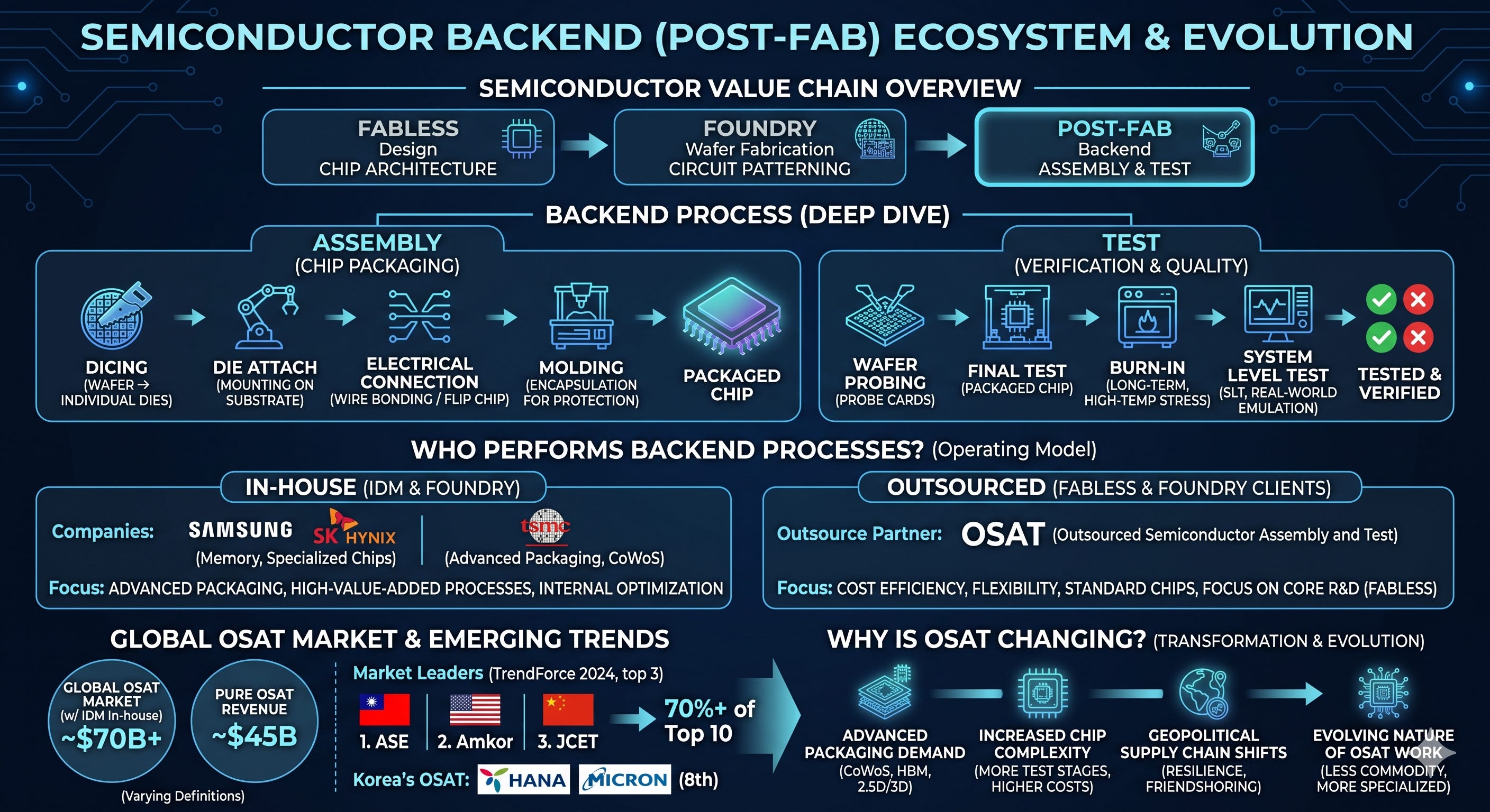
The semiconductor value chain broadly divides into design, manufacturing, and backend processing. Fabless companies design, foundries etch circuits onto wafers, and the final step turns those wafers into finished products through backend processing.
Backend processing splits into two categories. Assembly and test.
Assembly is the process of dicing wafers into individual chips, mounting them onto substrates (die attach), creating electrical connections (wire bonding or flip chip), and encapsulating them for protection from the external environment (molding). Only after these steps does a circuit on a wafer become a “chip.”
Test is the process of verifying that the finished chip operates as designed. It includes wafer probing at the wafer level, final test after packaging, burn-in under high temperature for extended periods, and SLT (System Level Test) that runs full inspection in actual system environments. As chips grow more complex, test stages multiply and costs rise.
Who handles this backend work? IDMs like Samsung and SK hynix package much of their own memory in-house, and TSMC directly handles high-value advanced packaging like CoWoS. But processing all backend in-house is inefficient. Investing tens of billions to install EUV equipment and develop 3nm processes versus dicing commodity chips and attaching them to substrates are fundamentally different in value-add. So a significant portion of backend is outsourced to specialists. These specialists are OSATs.
But right now, the nature of the work OSAT receives is changing. You need to understand why it’s changing now.
Why Now
OSAT was a commodity for decades. Why is it suddenly different? The answer lies in the physical structure of AI chips.
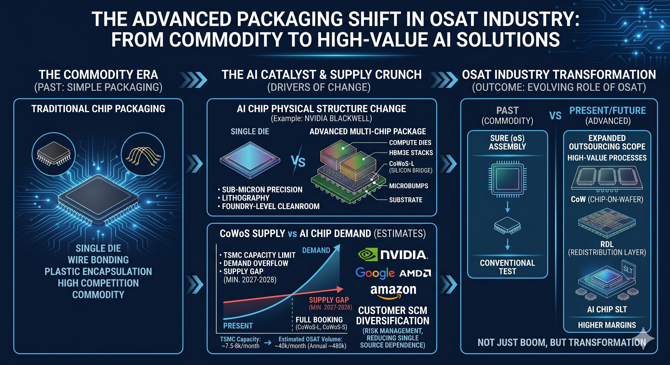
Traditional semiconductors had one die in one package. Wire bond it, wrap it in plastic, done. Any OSAT could do this, which is why it was a commodity.
AI GPUs are different. Take Nvidia Blackwell as an example. A single package contains 2 compute dies and 8 HBM3E stacks. Blackwell adopted CoWoS-L technology, which uses local silicon bridges instead of the conventional single silicon interposer (CoWoS-S).
Dies are connected through localized silicon bridges, bonded with microbumps, and mounted onto a substrate. This is a different dimension of technology from wire bonding. Whether interposer or bridge, connecting dies on silicon requires foundry-grade cleanrooms, lithography equipment, and sub-micron precision.
The problem is that extremely few can do this. CoWoS is a process that TSMC developed and TSMC dominates. But demand is exceeding TSMC’s capacity.
Industry estimates put TSMC’s CoWoS capacity at roughly 75,000 to 80,000 wafers per month currently, expanding to 120,000 to 130,000 by the end of 2026. Nvidia is estimated to account for more than half of global CoWoS demand, with AMD, Google, Amazon, and various custom ASIC players competing for the rest.
Reports indicate that both CoWoS-L and CoWoS-S lines are fully booked, suggesting demand substantially exceeds capacity. Building a new CoWoS line takes 18 to 24 months, so this gap will persist through at least 2027 to 2028.
The Age of the TSMC Bottleneck

In March 2026, Broadcom’s Natarajan Ramachandran stood in front of reporters and said something that would have been unthinkable a few years ago.
How does TSMC handle the excess? It hands it to OSAT. In the past, TSMC kept the high-value CoW (Chip-on-Wafer) bonding in-house and outsourced only the relatively lower-margin oS (on-Substrate) assembly and test to OSATs. But the demand surge has changed things. Recently, some CoWoS-related processes and comparatively simpler RDL structures have begun flowing to OSATs.
Some industry estimates even mention the possibility of expanded outsourcing of CoW-related processes. The scope of work OSAT receives is gradually widening. Sell-side estimates suggest CoWoS-related volume outsourced to OSATs reaches roughly 40,000 wafers per month (480,000 annually).
One more thing. Hyperscalers have begun voluntarily diversifying their supply chains. Nvidia, Google, and Amazon all want to reduce their 100% dependence on TSMC as a single source. Once an OSAT is qualified for CoWoS-related processes, customers allocate volume to OSAT directly, separate from what TSMC hands off. On top of the overflow from TSMC’s capacity shortage, there’s structural demand from customer risk management.
To sum up, the change happening in OSAT right now is not a simple cyclical upturn. The physical structure of AI chips has made advanced packaging mandatory, demand has exceeded what TSMC can handle alone, and the nature of the work OSAT receives is itself changing. Starting from oS assembly and gradually moving to higher-value processes, from conventional test to AI chip SLT. The quality of revenue is shifting.
Four Types of OSAT
Completely different businesses are running under the same OSAT label.
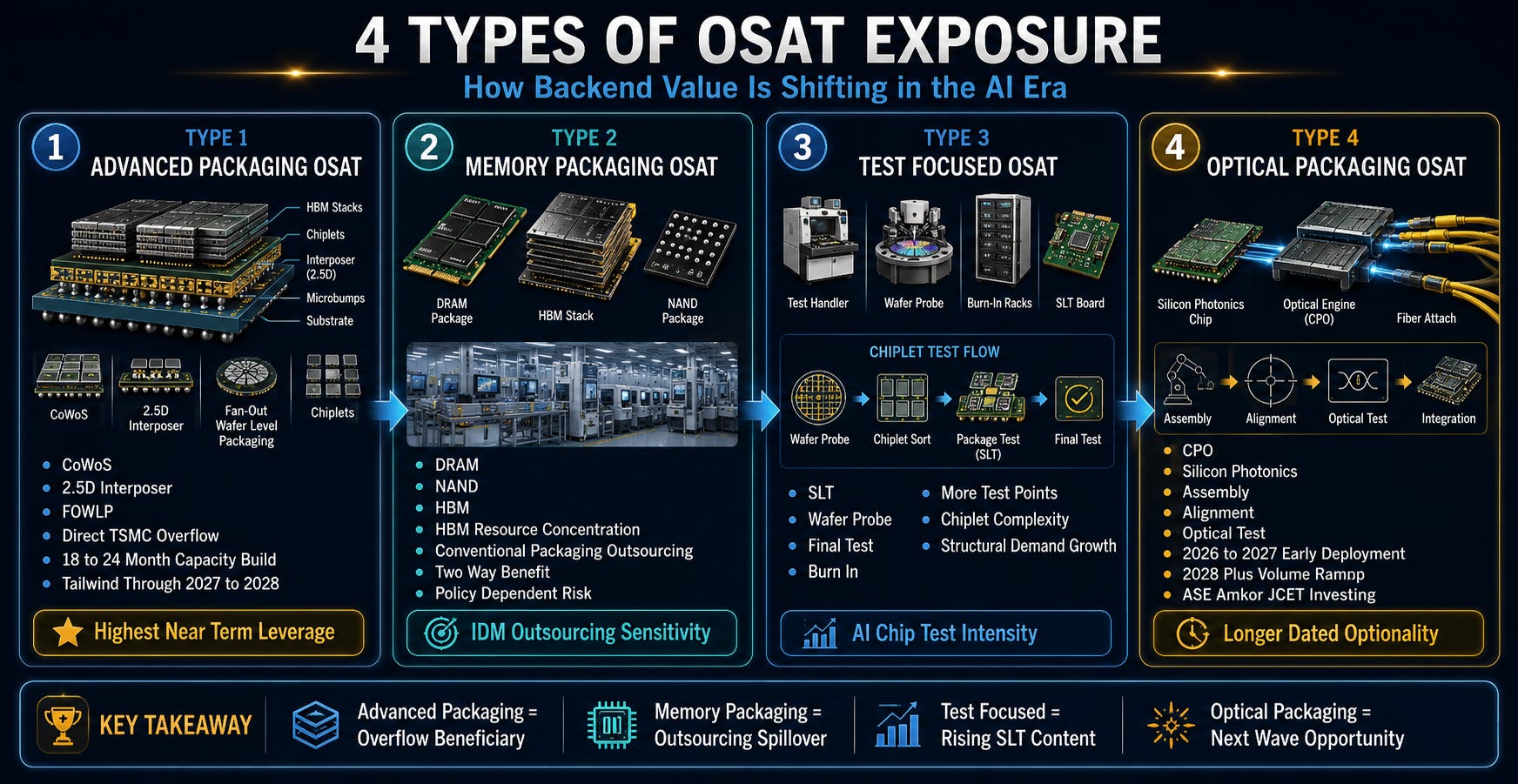
Type 1: Advanced Packaging OSAT
CoWoS, 2.5D interposer assembly, fan-out wafer-level packaging. Direct beneficiaries of TSMC overflow. Since new CoWoS lines take 18 to 24 months from groundbreaking to production, this tailwind is valid through at least 2027 to 2028.
Type 2: Memory Packaging OSAT
Backend processing for DRAM, NAND, and HBM. When resources concentrate on HBM, conventional DRAM/NAND packaging overflows to OSAT. A two-way beneficiary structure. The risk is dependency on IDM outsourcing policy.
Type 3: Test-Specialized OSAT
SLT (System Level Test) is the core. As chiplet architectures become standard, test points increase exponentially. SLT demand is growing structurally alongside rising AI chip complexity.
Type 4: Optical Packaging OSAT
Assembly, alignment, and test of CPO and silicon photonics chips. 2026 to 2027 is early deployment; volume production comes after 2028. ASE, Amkor, JCET, and some other global OSATs are currently investing in this capability.
This is why OSAT should no longer be viewed as a simple back end step in the AI semiconductor era.
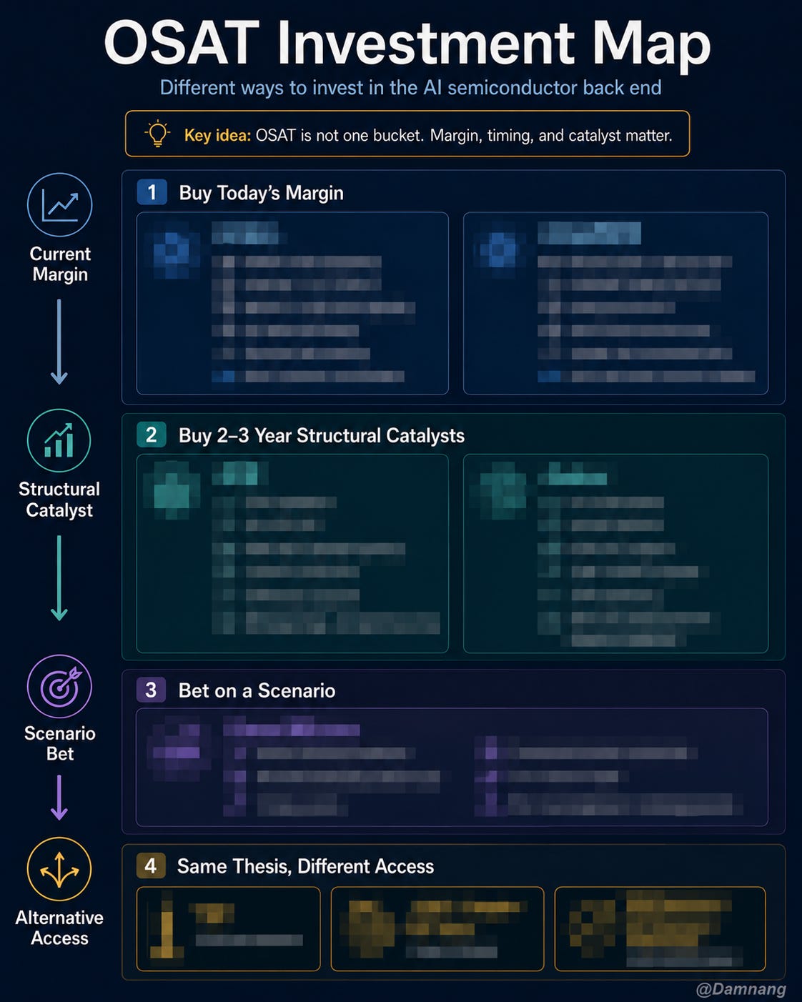
The key question is which OSAT companies are actually sitting at the bottleneck, which types of revenue can translate into higher margins, and which parts of the market are still underappreciated.
In the section below, I will focus on why OSAT margins can improve in the AI semiconductor era, where the market may still be missing the opportunity, and which companies deserve closer attention under this framework.