

In March 2026, Broadcom’s Natarajan Ramachandran stood in front of reporters and said something that would have been unthinkable a few years ago.
“Not long ago, you could have called TSMC’s capacity practically unlimited.
Today, in 2026, it’s the bottleneck choking the entire supply chain.”
From unlimited to bottleneck. This shift happened in just two to three years, and it wasn’t an accident. Yes, the explosion in AI demand played a role. But if you understand the structure of this industry, you can see exactly why everything converges on TSMC, and why switching to another foundry is not simply a matter of picking up and moving.
The TSMC bottleneck is an opportunity for Samsung and Intel. That part is true.
What most people get wrong is what kind of opportunity it actually is.
There’s a significant gap between what the market expects and what’s actually happening on the ground, and understanding that gap is what separates a good investment thesis from a bad one. This piece starts with how fabless companies and foundries actually work together, then moves to why customers can’t leave TSMC, where Samsung and Intel can realistically make money, and what conditions would have to hold for this dynamic to break.
In this piece:
How Chips Get Made: The Fabless-Foundry Relationship
Why TSMC Is So Hard to Catch
The Real Shape of the TSMC Bottleneck
Samsung Foundry: Where Things Actually Stand
What We Know and What We’re Estimating
The Taylor Fab: A $44B Bet, Up Close
What I’m Hearing on the Ground
My Take (Speculation Warning)
Intel Foundry: Where Things Actually Stand
What We Know and What We’re Estimating
Apple Is Coming Back to Intel
NVIDIA’s Feynman and Intel
The Risks Underneath the Good News
Where Intel Foundry Can Start Making Money: EMIB and “Made in USA”
What Betting on the “Not TSMC” Market Actually Means
Closing Thoughts
Disclaimer: All content in this article is based on my personal analysis of publicly available materials, press reports, analyst research, and industry networks. It is not based on any NDA-protected information from my current or former employers. This is not investment advice.
How Chips Get Made: The Fabless-Foundry Relationship
The most common misconception among investors new to semiconductors goes something like this:
“If TSMC is too expensive, why not just switch to Samsung or Intel?”
To answer that question, you first need to understand how a fabless company actually works with a foundry. The short answer is that switching foundries is not changing factories. It’s redesigning the chip from scratch.
Where Every Design Starts: The PDK
When a fabless company designs a chip, it does not start with a blank canvas. It starts on top of a PDK, or Process Design Kit, provided by the foundry.
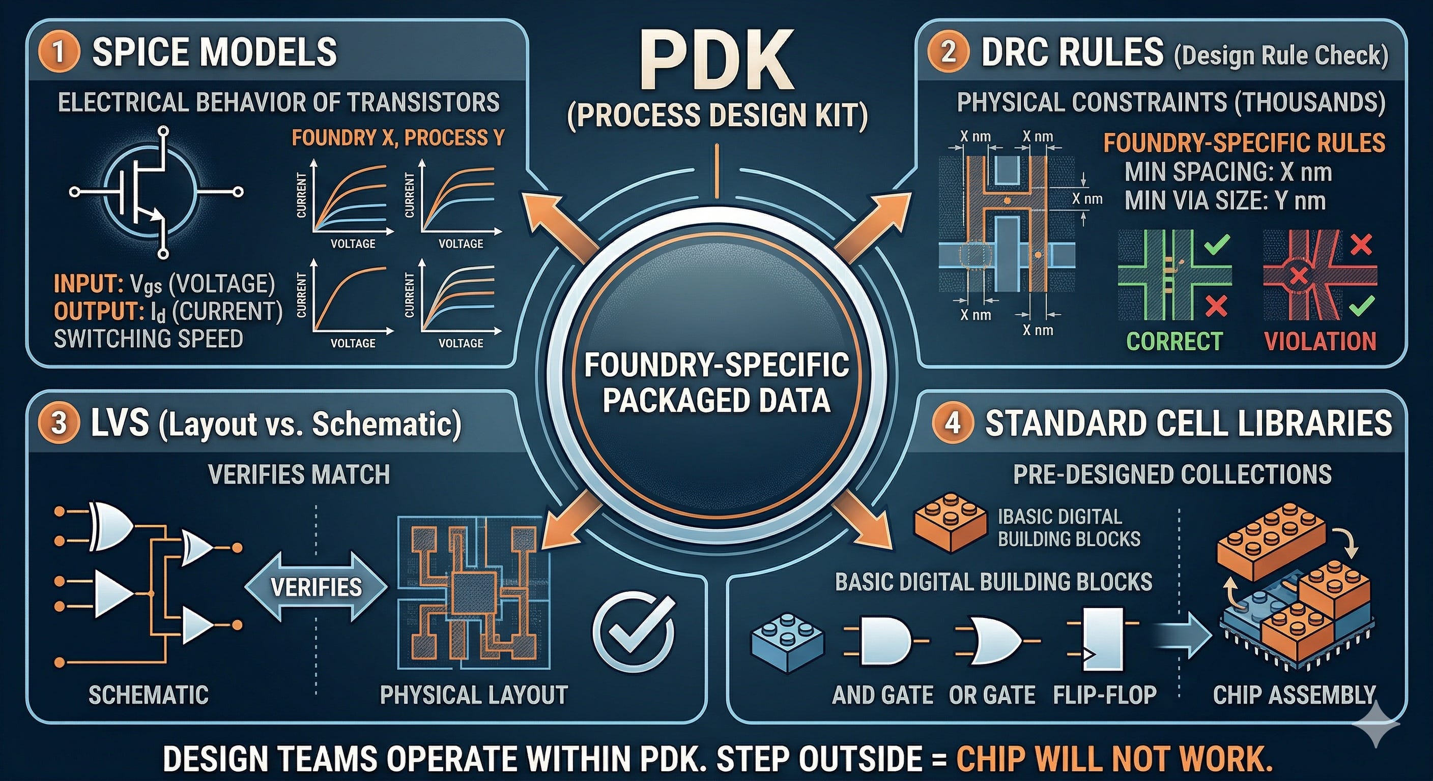
Let me explain concretely what a PDK contains. Every foundry runs a different process. The physical characteristics of transistors differ, the number and thickness of metal interconnect layers differ, the minimum spacing between devices differs. The PDK packages all of those differences into a form that a design team can actually use. Specifically, it includes the following.
SPICE models are mathematical descriptions of how each individual transistor behaves electrically. When a designer runs circuit simulations, these models tell you: “At this foundry, on this process, if you apply 1V to this transistor, here’s how much current flows and here’s the switching speed.” Change the foundry, and the models change entirely. Draw the same circuit and you get a completely different set of electrical characteristics.
DRC, or Design Rule Check, rules are physical constraints. Things like “minimum spacing between these two metal lines: X nanometers,” or “minimum via size: Y nanometers.” There are thousands of these rules. Violate them and you get shorts or opens in manufacturing. Every foundry uses different equipment and different lithography approaches, so every foundry has a different set of rules.
LVS, or Layout vs. Schematic, verifies that the physical layout a designer drew actually matches the intended circuit. Standard cell libraries are pre-designed collections of basic digital building blocks, AND gates, OR gates, flip-flops, all optimized for the specific process characteristics of that foundry. Designers assemble chips by combining these cells like Lego bricks.
Put it together and the PDK is everything you need to know to design a chip on that foundry’s process. Design teams operate entirely within the PDK. Step outside it and the chip either cannot be manufactured or will not work when it is.
So if you spent two years designing a chip on TSMC’s PDK and want to move it to Samsung Foundry, you have to redesign it from scratch on Samsung’s PDK. Different SPICE models means all simulations get re-run. Different DRC rules means all layouts get redrawn. Different standard cells means synthesis has to be redone. It’s a new project, full stop.
DTCO: When Design and Process Get Tangled Together
There’s a more recent development that makes this even harder. It’s called DTCO, or Design-Technology Co-Optimization.
For a long time, the sequence was: foundry develops the process, creates a PDK to match, hands it to the fabless customer, and the customer designs from there. Through 7nm and 5nm, that workflow mostly held.
At 3nm, and especially below 2nm, that sequence broke down. The transistor architecture itself shifted from FinFET to GAA, or Gate-All-Around, nanosheet structures, and design freedom and process constraints became far more deeply intertwined. For example, a wider nanosheet channel carries more current but reduces device density. A narrower channel gives you better density but less performance. These kinds of tradeoffs now get decided jointly between the design team and the process team from the very beginning of a project.
Metal stack configuration is the same story. An AI accelerator burning enormous amounts of power needs thick metal layers for efficient power delivery. A mobile AP prioritizes thin layers to shrink area. These choices get locked in at the start of the process, not at the end.
The result is that at 2nm and below, the option to “switch foundries later” has become dramatically more constrained. The chip’s architecture gets shaped around a specific foundry’s process characteristics early in the design phase. Moving to another foundry later means unwinding far more than it ever did in previous generations.
Tapeout: The $100M Decision You Cannot Take Back
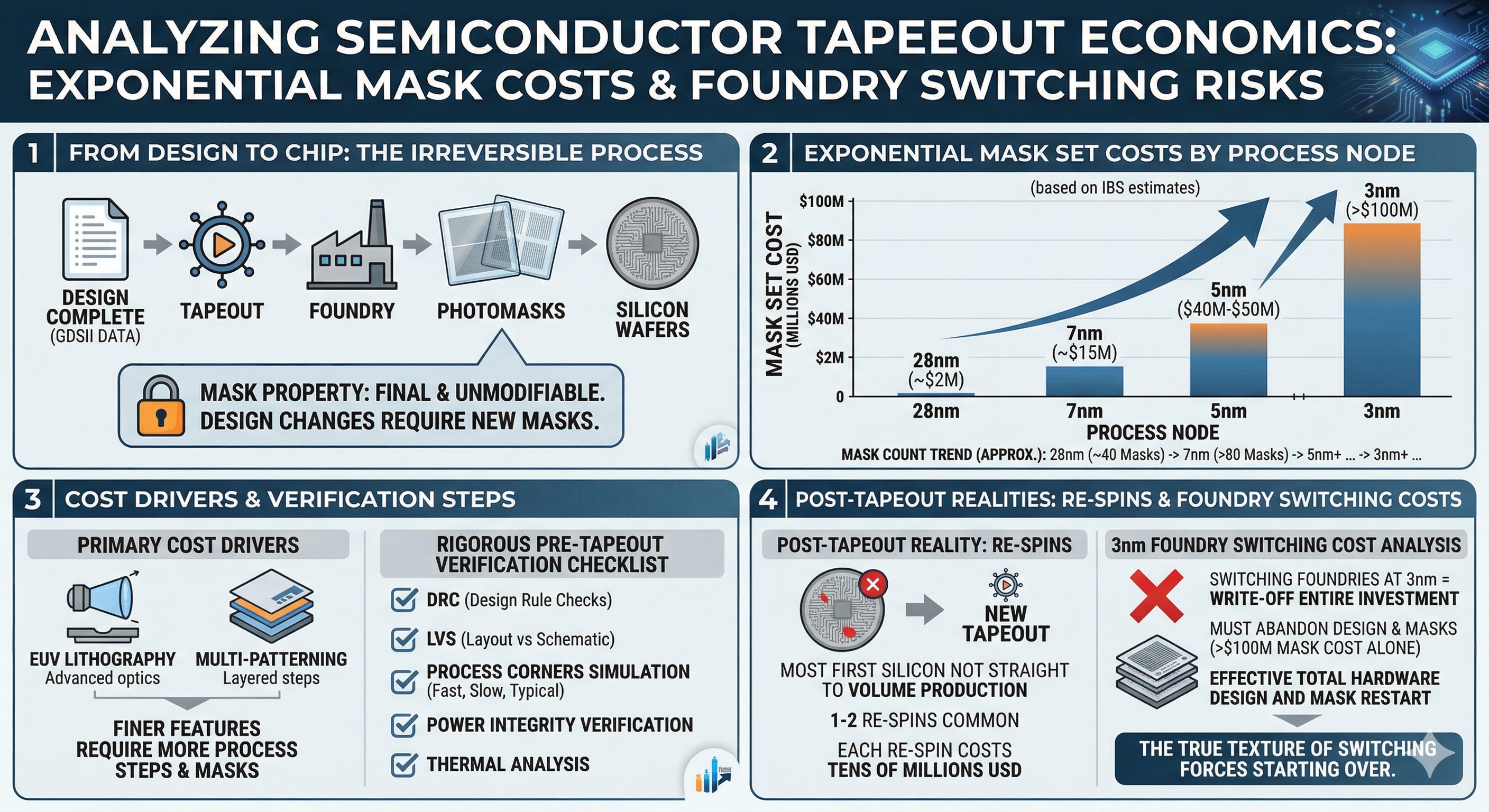
When a design is complete, it goes through tapeout. The finished design data, in GDSII format, gets handed to the foundry, which uses it to manufacture photomasks, the plates used to print circuit patterns onto silicon wafers. Once a mask is made, it cannot be modified. Change the design and you need new masks.
Mask costs scale dramatically with each new node. By IBS estimates, a mask set at 28nm runs about $2M. At 7nm it’s $15M. At 5nm, $40 to $50M. At 3nm, over $100M. The raw mask count tells the story: roughly 40 masks at 28nm, over 80 at 7nm. The increase comes from EUV lithography and multi-patterning, where printing finer features requires more process steps and therefore more masks.
Before tapeout, a design has to pass DRC, LVS, simulation across process corners (fast, slow, typical), power integrity verification, and thermal analysis. And even then, first silicon rarely goes straight to volume production. Most designs go through one or two re-spins, each costing tens of millions of dollars.
When a single tapeout at 3nm costs over $100M in masks alone, saying “I don’t like this foundry, let’s switch” means “let’s write off everything we’ve invested in design and masks and start over.” That is the real texture of switching costs.
Dual-Vendor Strategy: What I Saw Firsthand at Qualcomm
The natural follow-up question is: Why not run both foundries simultaneously?
Companies do.
When I was at Qualcomm, we ran Samsung and TSMC at the same time.
But what that actually involves is not what most people imagine. It is not “get quotes from two foundries and go with the cheaper one.” The process starts two to three years before launch, with parallel design work on both PDKs. Separate design teams are assigned to each, running simulations to compare PPA, which stands for Power, Performance, and Area, across both processes. You want to know which process delivers better numbers, and how timing margins differ when you run the same design through each.
Then you fabricate test chips at both foundries independently. When those come back, you measure silicon performance. Which foundry shows better model-to-hardware correlation? What are the yields? How many chips fall outside spec at certain process corners? This characterization work runs over two to three years, and only after enough data accumulates do you decide how to split the volume.
The only companies that can do this are Qualcomm, Apple, NVIDIA, the large-scale fabless players. You need the engineering headcount to run parallel design programs on two PDKs for multiple years simultaneously. For a smaller fabless company, dual-sourcing is not a realistic option. Pick a foundry and you’re committed for two to three years.
TSMC’s OIP: Locking In the Entire Ecosystem
TSMC has a program called OIP, or Open Innovation Platform, that maximizes this lock-in. It integrates EDA vendors like Synopsys and Cadence, IP vendors like ARM, and TSMC’s own packaging technologies like CoWoS and SoIC into a unified reference flow.
Why is this so powerful? The EDA tools a fabless company uses to design a chip need to be validated against the foundry’s PDK. Whether you’re using Synopsys Fusion Compiler for synthesis or Cadence Innovus for place-and-route, it only works well if a validated flow for that foundry’s PDK exists. TSMC works closely with major EDA vendors to release PDK-optimized reference flows first. IP vendors validate and release their IP on TSMC processes first.
For a fabless company, designing on TSMC’s OIP means EDA compatibility, IP validation, and packaging integration all come as a bundle. Using a different foundry means verifying every piece of that stack separately. If a particular IP block hasn’t been validated on that process, you wait for the IP vendor to do it. Intel 18A ran into exactly this problem, where IP validation delays slowed customer adoption.
Moving a chip designed within TSMC’s ecosystem to another foundry requires redesign work, IP re-validation, EDA flow reconstruction, and full timing re-verification. Technically possible. Practically, almost nobody does it. Switching foundries is not switching factories. It’s switching design infrastructure entirely. Once you’re on a PDK, two to three years of investment is locked in. That’s the first reason TSMC is hard to catch.
Why TSMC Is So Hard to Catch
PDK lock-in is only the starting point. TSMC’s moat is not a single wall. It’s layers stacked on layers.
The Yield Flywheel: Forty Years in Motion
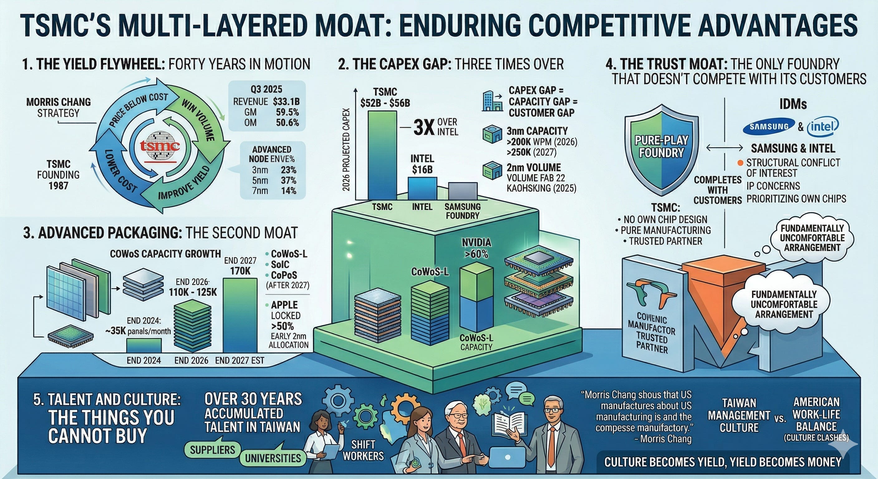
Morris Chang established a strategy during his time at TI that he carried into TSMC: stay ahead of the cost curve. Price below current cost to win volume, use that volume to improve yield, let yield improvement drive cost down, use lower costs to attract more customers. A flywheel.
TSMC has been spinning that flywheel since its founding in 1987. As of Q3 2025, quarterly revenue was NT$989.92 billion (roughly $33.1B), up 30.3% year-over-year, with gross margin of 59.5% and operating margin of 50.6%. The 3nm node accounted for 23% of wafer revenue, 5nm 37%, and 7nm 14%. Advanced nodes below 7nm together represent 74% of total wafer revenue.
What those numbers tell you is simple. TSMC is the only foundry that can make money on advanced nodes and reinvest it into the next generation at the same time.
The Capex Gap: Three Times Over
TSMC’s annual capex for 2026 is estimated at $52 to $56 billion. Intel’s is $16 billion. TSMC is building more than three Intels every year. Samsung Foundry’s capex runs even lower.
On 3nm capacity alone, TSMC is targeting over 200,000 wafer starts per month by end of 2026, expanding toward 250,000 by 2027. Volume production on 2nm started at Fab 22 in Kaohsiung in Q4 2025, with additional phases under construction. In a capital-intensive industry, a capex gap is a capacity gap, and a capacity gap is a customer gap.
Advanced Packaging: The Second Moat
TSMC’s advanced packaging capabilities have emerged as another major competitive advantage. CoWoS capacity is projected to expand from roughly 35,000 panels per month at end of 2024 to between 110,000 and 125,000 by end of 2026, with some estimates reaching 170,000 by end of 2027. CoWoS-L, SoIC, and CoPoS slated for introduction after 2027 all point to TSMC maintaining its lead on the packaging roadmap as well.
By analyst estimates, NVIDIA holds over 60% of CoWoS-L capacity, and Apple has locked in more than half of early 2nm allocation. When you factor in packaging, the exits from TSMC’s ecosystem shrink to almost nothing.
The Trust Moat: The Only Foundry That Doesn’t Compete With Its Customers
There’s one more structural advantage embedded in TSMC’s business model. It’s a pure-play foundry. TSMC designs no chips of its own. It never competes with its customers.
Samsung is different. Samsung designs Exynos APs for its own Galaxy smartphones while simultaneously manufacturing Qualcomm’s Snapdragon. From a customer’s perspective, handing over critical IP to a direct competitor is a fundamentally uncomfortable arrangement. This structural conflict of interest is Samsung Foundry’s chronic trust problem.
Intel faces the same issue. An IDM running its own CPUs while offering to manufacture chips for outside customers invites the obvious concern: won’t Intel prioritize its own chips over mine?
Talent and Culture: The Things You Cannot Buy
Morris Chang once said that American semiconductor manufacturing is “a very expensive exercise in futility.” It sounds harsh, but it’s not wrong. Taiwan has over thirty years of accumulated manufacturing talent. Suppliers, universities, shift workers, every layer of the stack is precisely calibrated around a single mission: manufacturing the best chips in the world. You can build a fab with money. You cannot buy the knowledge that lives inside it.
There was substantial reporting on culture clashes at TSMC’s Arizona fab, where American engineers’ expectations around work-life balance ran headlong into the Taiwanese management culture of unconditional commitment. This is not just an HR problem. In manufacturing, culture becomes yield, and yield becomes money.
TSMC’s moat is not a single technology. It’s the yield flywheel, the scale, the ecosystem, the packaging, the trust, and the culture, all stacked on top of each other. Catching up on any one of them does not mean much on its own.
And yet, in 2026, two variables have emerged that could actually move this dynamic.
One is Samsung’s memory business.
Starting with HBM4, the base die at the bottom of the DRAM stack needs to be manufactured on an advanced foundry process. Samsung is the only company in the world that owns DRAM, logic foundry, and packaging all under one roof, and it is now actively turning that vertical integration into a foundry customer pitch.
How Samsung Overtakes SK hynix in HBM4: An ISSCC 2026 Paper Review

This article is based on the paper “A 36GB 3.3TB/s HBM4 DRAM with Per-Channel TSV RDQS Auto Calibration and Fully-Programmable MBIST” presented by Samsung Electronics at ISSCC 2026. This is a review written with the author’s permission, explaining the paper’s key points from a reader’s perspective and adding personal interpretation.
The other is Intel’s EMIB.
With TSMC’s CoWoS in short supply, Intel’s advanced packaging technology is emerging as the only real alternative at scale. The reports that NVIDIA’s next-generation Feynman chip will use EMIB are a signal that the packaging competition is entering a new phase.
EMIB: Intel Foundry's Best Hope

The bottleneck in the semiconductor industry has shifted. For a long time, almost everything came down to how small you could make a transistor. That’s no longer the whole story. Increasingly, what matters is how fast and efficiently you can connect multiple chips inside a single package. Packaging has become a critical competitive axis.
How these two variables are creating real opportunities for Samsung and Intel in the TSMC bottleneck era, drawing on what I’m hearing on the ground, is what the rest of this piece covers.