

These days, you can’t have a conversation about semiconductors or AI infrastructure without CPO (Co-Packaged Optics) coming up.
“The optical era is here.”
“CPO is replacing pluggable.”
“Buy the silicon photonics beneficiaries.”
X(Twitter), YouTube, sell-side reports. Everyone’s shouting about CPO.
But let me ask you something. Do you actually know what CPO is?
I get these questions all the time.
“When CPO takes over, aren’t all the pluggable companies dead?”
“Once optical interconnect arrives, doesn’t HBM become irrelevant?”
Both questions come from the same kind of misunderstanding. People compress a technology trend into a single headline, then skip over everything that actually matters underneath it.
Miss these distinctions and your investment thesis is wrong from the start.
Sure, stock prices move on expectations regardless of technology maturity, and markets always love the simple narrative that “this kills that.” But the actual industry doesn’t work that way.
A months ago, when Hock Tan said copper was still the workhorse, the market interpreted it as “CPO is dead” and dumped optical stocks across the board. If you don’t know where the technology actually sits, you can’t tell the difference. And for investors who did know the coordinates, that selloff was an opportunity..
This article will separate four things. The direction of the technology. The current coordinates. Market expectations. The actual monetization timeline. When all four align, you go in with conviction. When they don’t, the gap is either an opportunity or a trap.
1. What CPO Actually Is: Why It’s Inevitable in Both Scale-up and Scale-out
In one sentence, CPO means putting the optical engine (the component that converts electrical signals to light) inside the same semiconductor package as the switch chip or GPU. Instead of electrical signals traveling tens of centimeters across copper PCB traces to reach a pluggable module on the front panel, they travel just a few millimeters inside the package before converting to light.
To understand why this matters, you need to separate two domains of data center interconnect.
![Why CPO Is Becoming Inevitable? [CPO Special Part 1]](https://substackcdn.com/image/fetch/$s_!9bf7!,w_1300,h_650,c_fill,f_webp,q_auto:good,fl_progressive:steep,g_auto/https%3A%2F%2Fsubstack-post-media.s3.amazonaws.com%2Fpublic%2Fimages%2F30766732-0379-47eb-bc82-ff73fa8b10d1_900x491.jpeg)
Scale-up: Direct GPU-to-GPU Communication. Currently 100% Copper. But the Wall Is Visible.
Scale-up is the interconnect that ties tens to hundreds of GPUs together into what behaves like one massive GPU. At NVIDIA, NVLink handles this. During AI model training, the model is split across multiple GPUs, and data flows constantly between them. You need extreme bandwidth (3.6TB/s per GPU in the Rubin generation) and extreme low latency. Distances are short. Everything happens within a rack. This domain is 100% copper cable today.
Tracking NVIDIA’s roadmap generation by generation shows exactly where copper starts hitting limits.
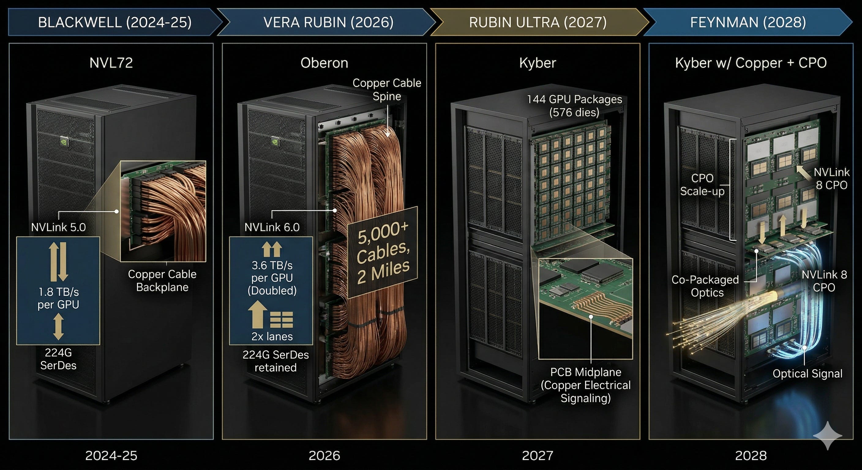
Blackwell (2024-25): NVLink 5.0, 1.8TB/s per GPU, copper cable, NVL72 rack.
Vera Rubin (2026): NVLink 6.0, 3.6TB/s per GPU, doubled. The key detail: they didn’t increase lane speed. They doubled the number of lanes (keeping 224G SerDes). The Oberon rack copper spine carries 5,000+ cables, total length 2 miles. Still copper.
Rubin Ultra (2027): Kyber rack. 144 GPU packages (576 GPU dies) in a single NVLink domain. A PCB midplane replaces cables, but this is still copper-based electrical signaling.
Feynman (2028): This is where the shift happens. At GTC 2026, Jensen said it: “Feynman has Kyber with copper and CPO scale-up.” NVLink 8 CPO enters scale-up for the first time.
Why is copper hitting a wall?
There are really only two ways to increase data bandwidth.
One is to make each lane faster. The other is to add more lanes. The industry has mostly relied on the first approach, pushing lane speed higher.
The problem is that this approach is running into physics.
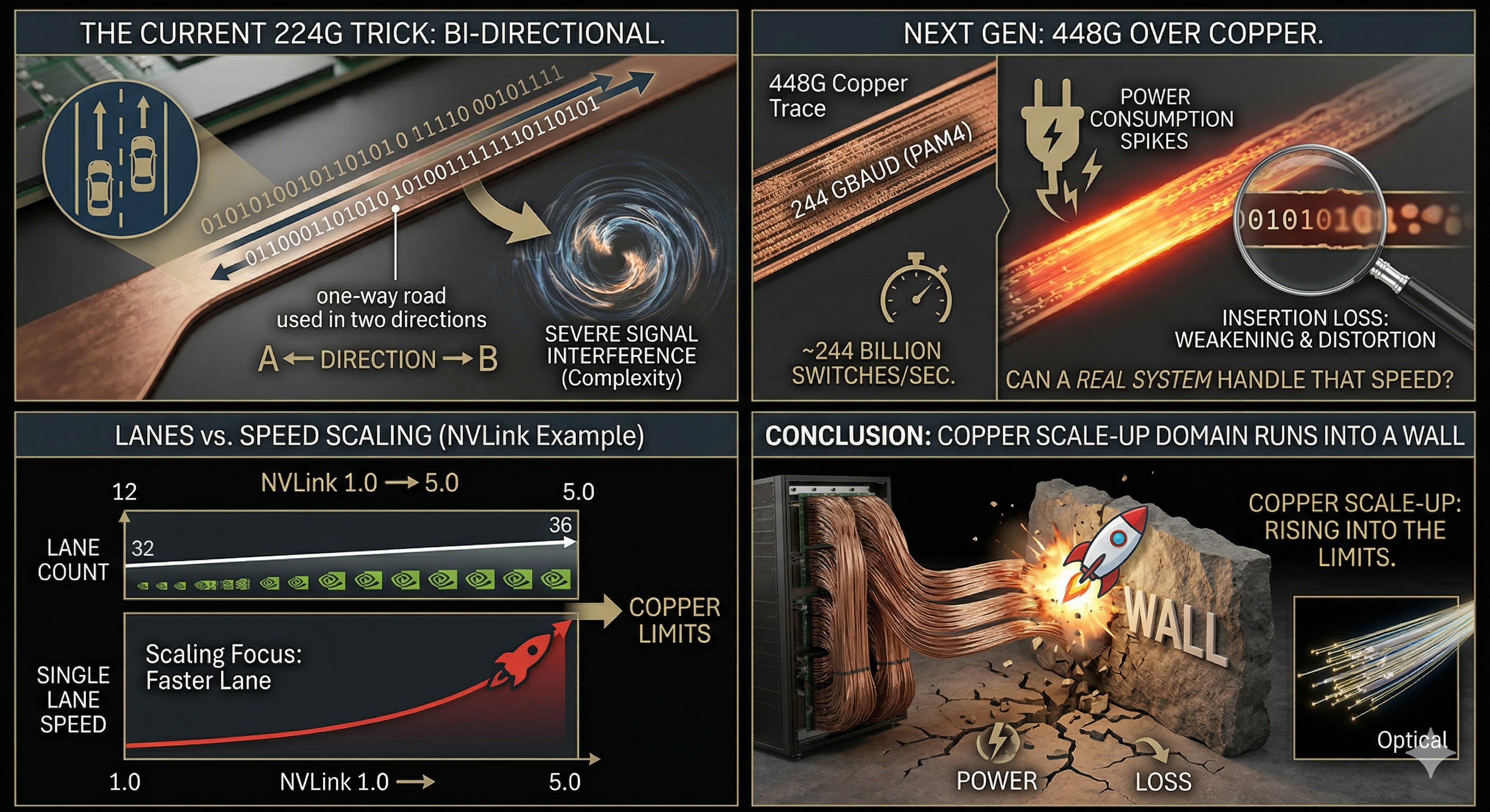
At the current 224G SerDes, the industry uses bi-directional transmission, sending data both ways on the same trace simultaneously, effectively doubling bandwidth. Think of it as using a one-way road in both directions at once. But this introduces severe signal interference and implementation complexity. You can pull it off once, but repeating the trick for the next generation is a different story.
Moving to 448G SerDes makes things far worse.
Doing this over copper requires roughly 244 GBaud in PAM4, meaning the signal state has to switch about 244 billion times per second. At that speed, you can’t just build a better circuit. Power consumption spikes, and insertion loss (the weakening and distortion of signals as they travel through copper traces, packages, and boards) becomes overwhelming. The real question stops being “can we make it faster” and becomes “can a real system handle that speed.”
Adding more lanes isn’t straightforward either.
Look at NVLink. From version 1.0 to 5.0, the lane count barely moved, from 32 to 36. Almost all the bandwidth gains came from pushing each lane faster. And if lane speed is now approaching physical limits, copper-based scaling can’t keep going the way it has.
The bottom line: copper in the scale-up domain is running into a wall.
The industry has brute-forced its way through so far, but we’re entering territory where simple engineering optimization won’t cut it.
Scale-out: Network Communication. Currently Pluggable. But the Power Wall Is Coming.
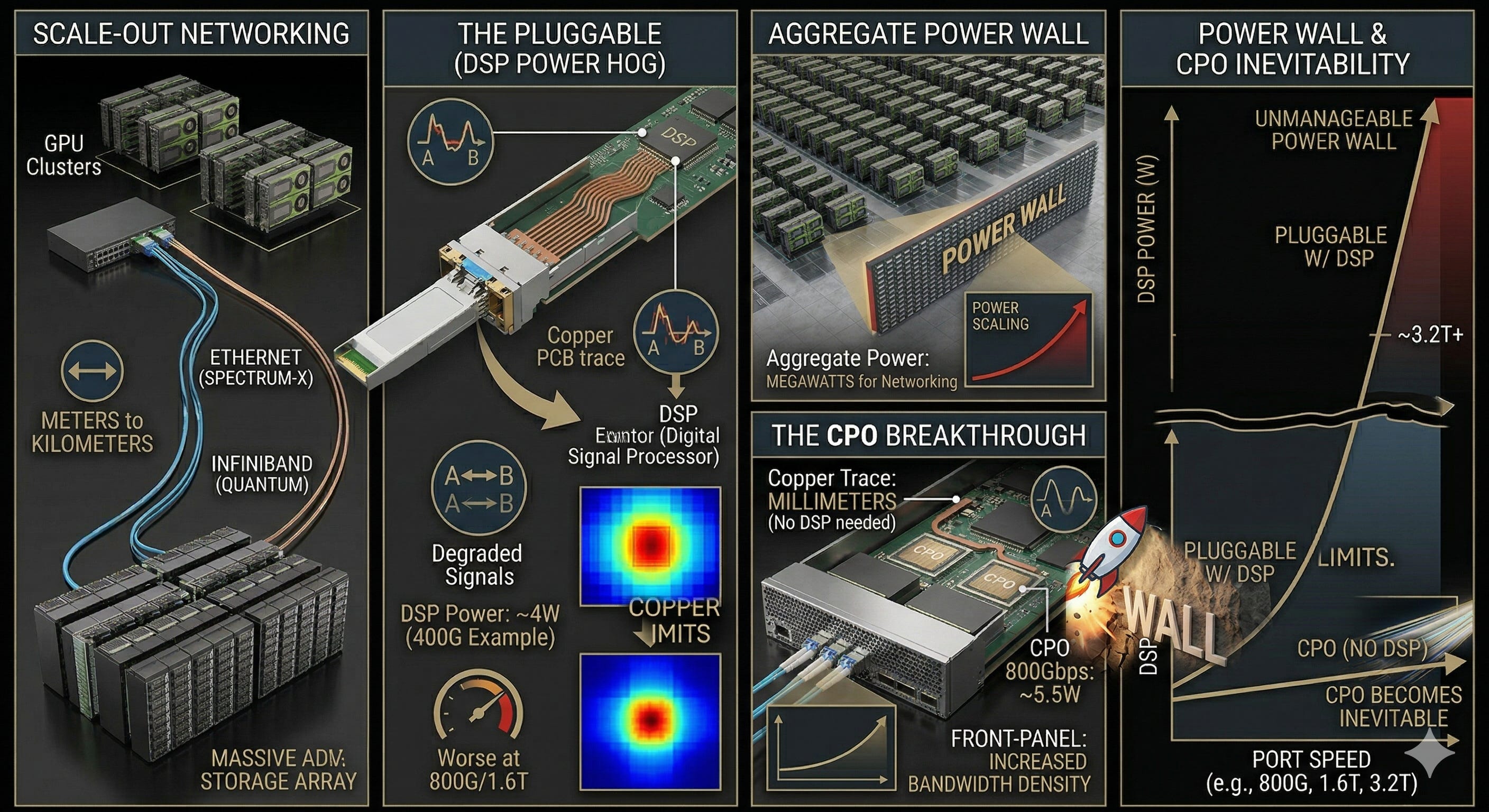
Scale-out covers network communication between different GPU clusters and between GPUs and storage. Ethernet (NVIDIA Spectrum-X) or InfiniBand (NVIDIA Quantum) handles this. Distances are longer (meters to kilometers). Pluggable optical transceivers dominate here. These are hot-swappable modules that plug into the switch front panel, converting electrical signals to light and sending them over optical fiber.
Inside every pluggable sits a DSP (Digital Signal Processor). High-speed electrical signals from the switch chip travel tens of centimeters across copper PCB traces and get weakened and distorted along the way. The DSP digitally cleans them up. The problem: DSPs are power hogs. In a 400G module, the DSP alone consumes about half the total power (around 4W). At 800G and 1.6T, it’s worse.
Why does scale-out need CPO? Data center power budgets aren’t infinite. GPUs eat most of the rack power. Networking eats the rest. As GPU counts grow, the number of pluggable transceivers explodes, and the aggregate DSP power becomes impossible to ignore. A 128,000-GPU cluster needs hundreds of thousands of pluggable, each pulling 10 to 15W. Add it up and you’re talking megawatts.
CPO eliminates the DSP entirely. The copper trace shrinks to a few millimeters, so signal conditioning becomes unnecessary. Broadcom’s numbers: 800Gbps port, pluggable 15W vs. CPO 5.5W. Roughly a 3x difference. The front-panel pluggable slots disappear too, increasing bandwidth density.
In scale-out, CPO is the technology that breaks through the power wall. At 800G, pluggable works fine. But at 3.2T and beyond, DSP power becomes unmanageable. That’s when CPO becomes inevitable.
Summary: CPO Is Inevitable in Both Domains, but for Different Reasons
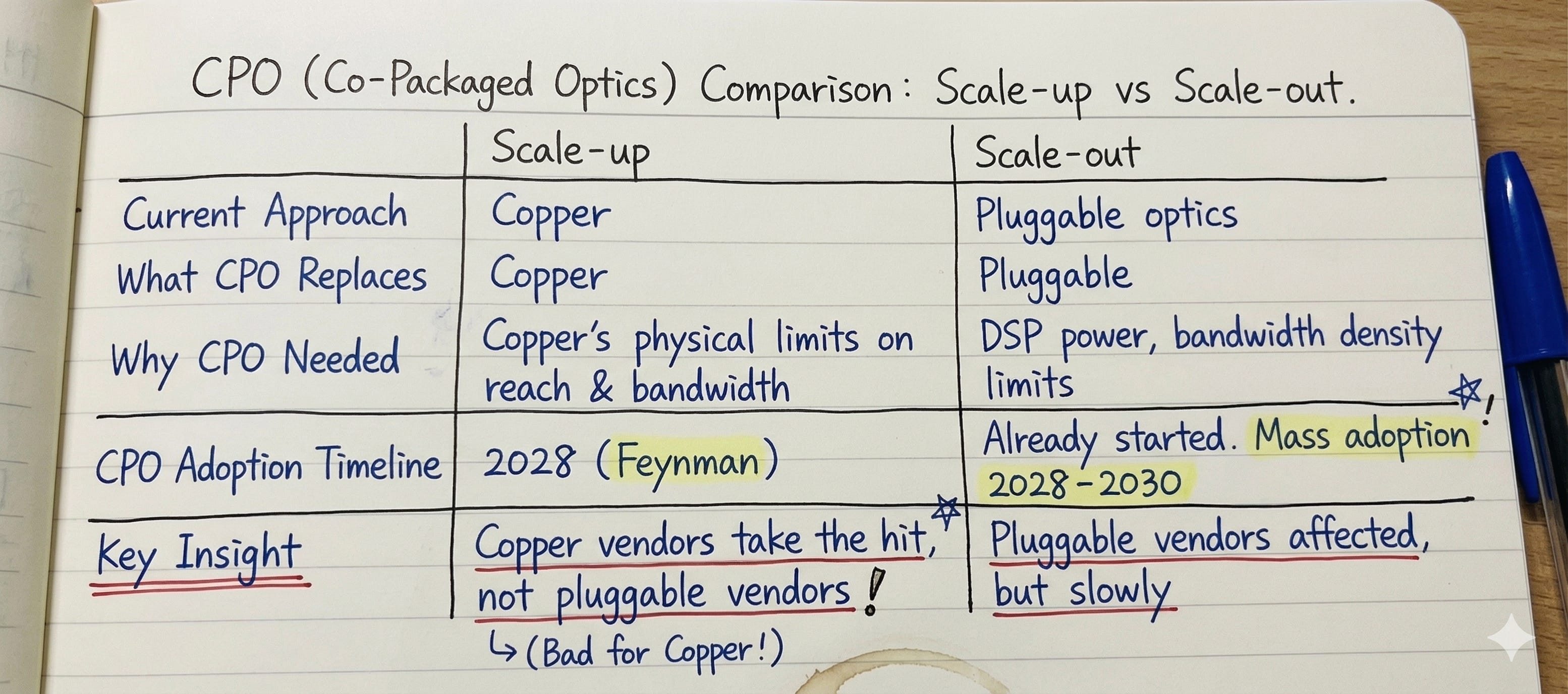
So everyone’s racing in.
NVIDIA announced Spectrum-X Photonics (Ethernet CPO switch) and Quantum-X Photonics (InfiniBand CPO switch) at GTC 2025, then declared Spectrum-X CPO “full production” at GTC 2026.
Broadcom built the Bailly CPO switch, integrating 8 optical engines into a Tomahawk 5 switch chip for 51.2Tbps, making it the industry’s first volume production CPO switch.
Marvell acquired Celestial AI for $3.25B, the company whose silicon photonics technology disaggregates memory and compute over light, signaling ambitions well beyond simple transceivers into full AI architecture redesign.
Startups are pouring in.
Ayar Labs closed a $500M Series E three weeks ago with NVIDIA and MediaTek participating, bringing cumulative funding past $2.6B.
Lightmatter took its photonic fabric approach (laying photonic interconnect underneath the chip) to a $4.4B valuation.
The direction is clear.
The problem is that direction being right doesn’t mean it works today.
2. Why CPO Can’t Enter Scale-up Yet
I said CPO is inevitable in scale-up.
That’s true. But NVIDIA is sticking with copper through 2028 for good reasons. The technical mountains between here and scale-up CPO are tall.
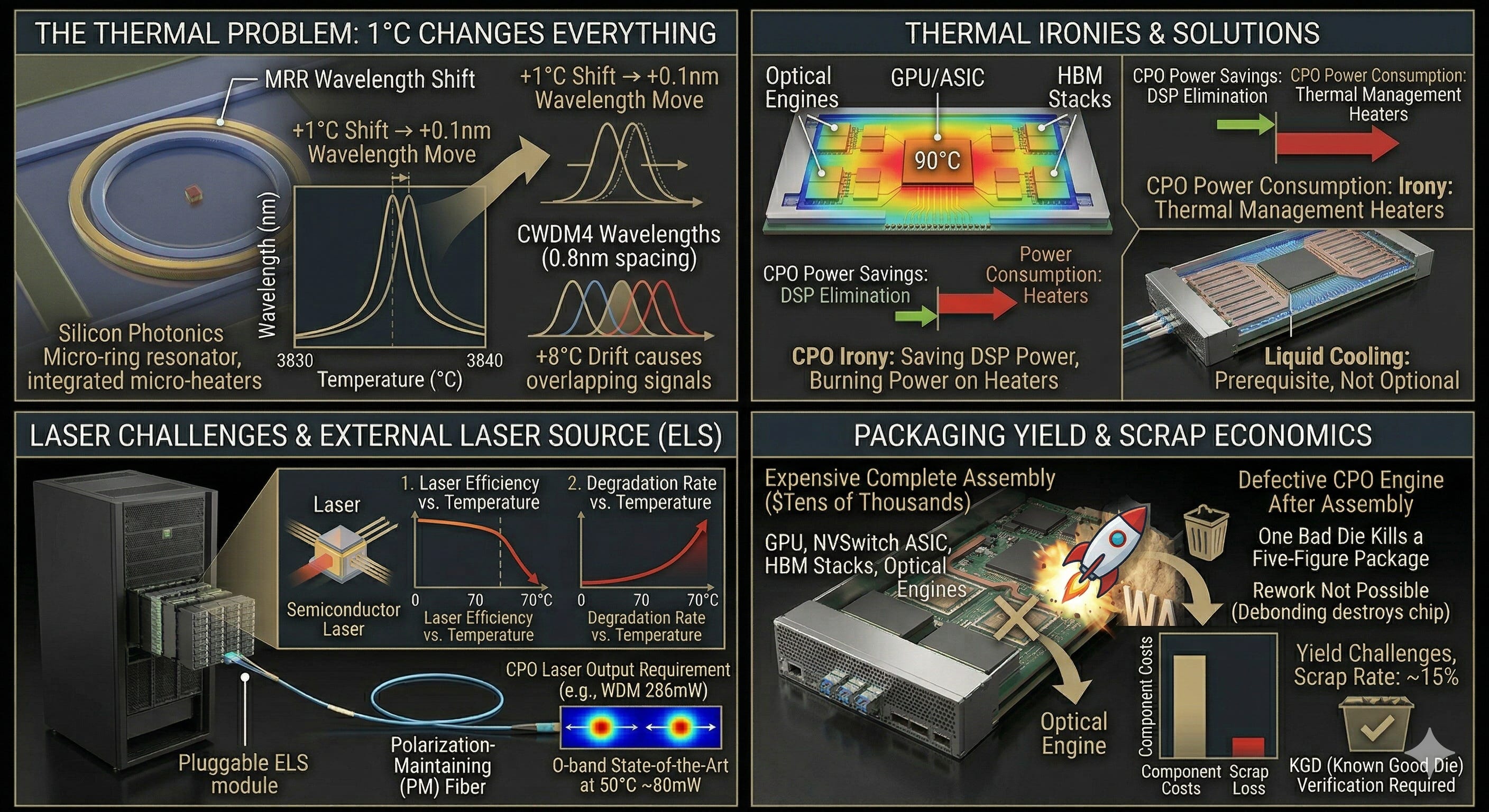
The Thermal Problem: 1°C Changes Everything
Inside a scale-up package sits a GPU or NVSwitch ASIC. These chips run at 90°C or higher. CPO means putting optical engines inside the same package.
Silicon photonics widely uses micro-ring resonators (MRR), tiny ring-shaped structures that pass only specific wavelengths of light. MRRs are extremely sensitive to temperature. A 1°C shift moves the resonant wavelength by about 0.1nm. In WDM, where channel spacing is 0.8nm (CWDM4), just 8°C of drift can cause adjacent channels to overlap. Maintaining this level of precision next to an ASIC running at 90°C is an extreme challenge.
To compensate, you need individual heaters on each MRR for precise thermal control. But those heaters consume power. The irony: CPO saves power by eliminating DSPs, then potentially burns it right back on thermal management. Liquid cooling isn’t optional for CPO. It’s a prerequisite.
Lasers make the thermal problem even worse. Semiconductor lasers lose efficiency rapidly above 70°C and suffer accelerated degradation. The industry standard is ELS (External Laser Source), placing the laser outside the package. An ELS plugs into the switch front panel, generates CW light (unmodulated, pure light), and sends it via fiber to the PIC inside the package. It’s a sensible approach, but it requires polarization-maintaining fiber (specialized fiber that preserves light’s polarization state), which adds fiber routing complexity and insertion loss. CPO lasers need far higher output than pluggable lasers (286mW for WDM, at least 100mW for DR). Current state of the art in O-band at 50°C tops out around 80mW.
Packaging Yield: One Bad Die Kills a Five-Figure Package
A scale-up CPO package contains a GPU or NV Switch ASIC, HBM stacks, and multiple optical engines, all on one substrate. This package costs tens of thousands of dollars. If a single optical engine turns out defective after assembly? Scrap the entire thing. Rework isn’t possible. Debonding optical components destroys the chip.
So you need KGD (Known Good Die) verification before assembly, meaning every die must be confirmed good beforehand. But wafer-level optical testing for silicon photonics is still in its infancy (more on this in Section 4). Analyses suggest packaging yield struggles to break past 85%. In scale-up, where package prices are this high, a 15% scrap rate destroys the economics.
Copper Is Still Cheap and Proven
Copper DAC costs more than 10x less than optical alternatives.
Latency is sub-nanosecond (no electrical-to-optical conversion needed).
Reliability is backed by 20+ years of field data. If a connector comes loose, you just push it back in. CPO has to clear every one of the technical hurdles above before it can beat that kind of simplicity and proven stability.
Broadcom CEO Hock Tan first introduced CPO to the world at J.P. Morgan in 2021. But in Broadcom’s March 2026 earnings call, he said: “We’re not quite there yet.” Copper is still the scale-up mainstay, and silicon photonics is progressing through 400G to 800G to 1.6T development stages. The man who brought CPO into the spotlight personally said “not yet.”
At GTC 2026, Jensen put it this way: “Is copper still important? Yes. Are we doing scale-up optical? Yes. We need more copper, more optics, more CPO.” Not the death of copper. Coexistence. At least through 2028.
3. Scale-out: CPO Has Launched, but Pluggable Isn’t Going Down Easy
Scale-out is a different story. CPO products already exist here.
But SemiAnalysis puts it bluntly: scale-out CPO’s TCO advantage isn’t “compelling enough for customers to dive headfirst into an entirely different deployment paradigm.”
The title of Cignal AI’s February 2025 report says it perfectly: “Inevitable but Not Imminent.” Mass deployment is 3 to 5 years away.
Why? Because the pluggable camp isn’t standing still.
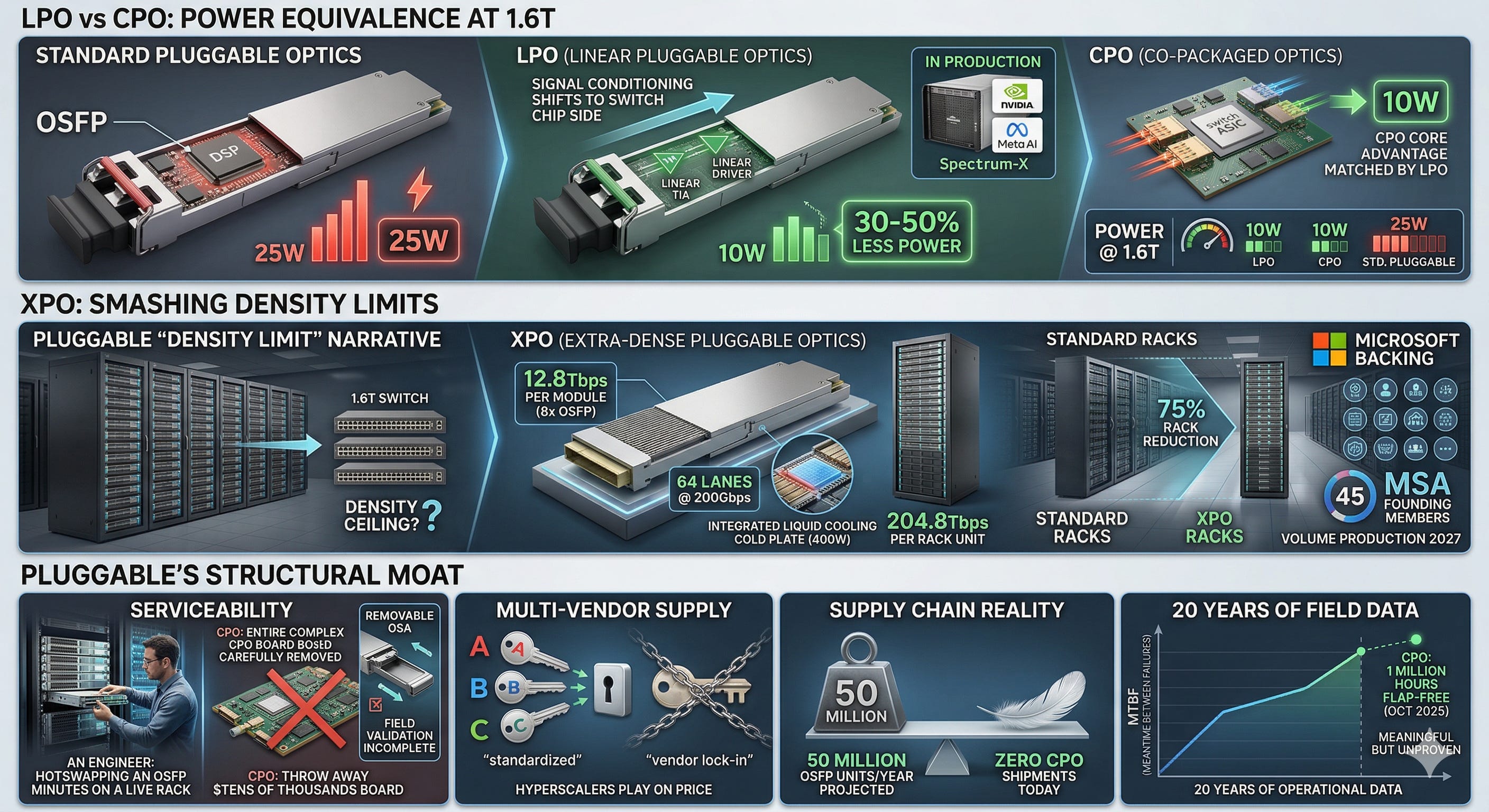
LPO: Stripping Out the DSP to Close the Power Gap
LPO (Linear Pluggable Optics) removes the DSP from inside the pluggable module. Signal conditioning shifts to the switch chip side, leaving only analog components (linear TIA, linear driver) in the module. Same pluggable form factor, but 30 to 50% less power. Already deployed in production at NVIDIA Spectrum-X and Meta’s AI network.
Data from Arista’s Andy Bechtolsheim, presented at OFC 2025. At 1.6Tbps: DSP pluggable 25W, CPO and LPO each around 10W. At the 1.6T generation, LPO and CPO are essentially power-equivalent. CPO’s core selling point, power savings, gets nearly matched by pluggable just by removing the DSP. So why take on the added complexity of CPO?
XPO: Demolishing the Density Argument Too
Ten days ago at OFC 2026, Arista unveiled XPO (eXtra-dense Pluggable Optics). A direct counter to the CPO camp’s claim that pluggable has a density ceiling.
12.8Tbps per module (8x OSFP). 64 lanes at 200Gbps. 204.8Tbps per rack unit (4x OSFP). Integrated liquid cooling cold plate (400W per module). 45 founding members in the MSA, with Microsoft backing. Volume production targeted for 2027.
In a 400MW data center with 128,000 GPUs: over 1,400 OSFP switch racks would drop by 75% with XPO. The pluggable “density limit” narrative starts to crumble.
Pluggable’s Structural Moat
Even if CPO is technically superior, pluggable has structural advantages that don’t go away easily.
Serviceability: A pluggable fails, you pull the module and plug in a new one. Takes minutes. CPO means swapping the entire board. You’re throwing away a package worth tens of thousands of dollars. NVIDIA designed a removable OSA for Quantum-X CPO, but field validation isn’t complete.
Multi-vendor supply: The OSFP MSA has dozens of member companies. Hyperscalers buy the same spec module from multiple vendors and play them against each other on price. CPO means vendor lock-in. That’s the structure hyperscalers hate most.
Supply chain reality: “Current CPO shipment volume is zero. Next year’s projected OSFP shipments are 50 million units. Going from zero to 50 million is not possible.”
20 years of field data: Pluggable MTBF and failure modes are thoroughly understood. CPO’s biggest achievement so far is Broadcom plus Meta’s “1 million hours flap-free” result from October 2025. Meaningful, but it doesn’t compare to two decades of operational data.
When Does Scale-out CPO Hit Mass Adoption?
800G: pluggable handles it fine.
1.6T: LPO and XPO extend pluggable’s life.
3.2T+ (the 400G-per-lane generation): DSP power and insertion loss push past what pluggable can handle.
That’s the inflection. Timing? 2028 to 2030.
4. The Real Bottlenecks to CPO Commercialization
4-1. Silicon Photonics Manufacturing: Light Demands 1nm Precision
The core component of CPO is the PIC (Photonic Integrated Circuit). Think of it as a semiconductor chip that handles light instead of electrons. It contains waveguides (channels that carry light), modulators (components that encode data onto light), photodetectors (components that convert light back to electrical signals), and more, all integrated on a single chip.
A standard logic chip (CPU, GPU) can tolerate some variation in transistor characteristics. It’s digital. As long as it can tell “1” from “0,” it works. PICs are different. If a waveguide’s thickness is off by just 1nm, the light propagation changes, the modulator’s operating wavelength shifts, and you end up with data errors. Like a water pipe where even 0.01mm of diameter variation alters the pressure and flow. Analog-level precision is non-negotiable.
The big promise of silicon photonics is that you can make PICs in CMOS fabs, leveraging existing semiconductor equipment. But the process requires steps that don’t exist in standard CMOS flows: depositing Ge (germanium) photodetectors, forming SiN (silicon nitride) waveguide layers, bonding III-V laser material. The yield of these additional steps determines the entire PIC yield.
That’s why “who makes the PIC” is the starting point of the entire CPO ecosystem. Three foundries are competing, each with a different approach.
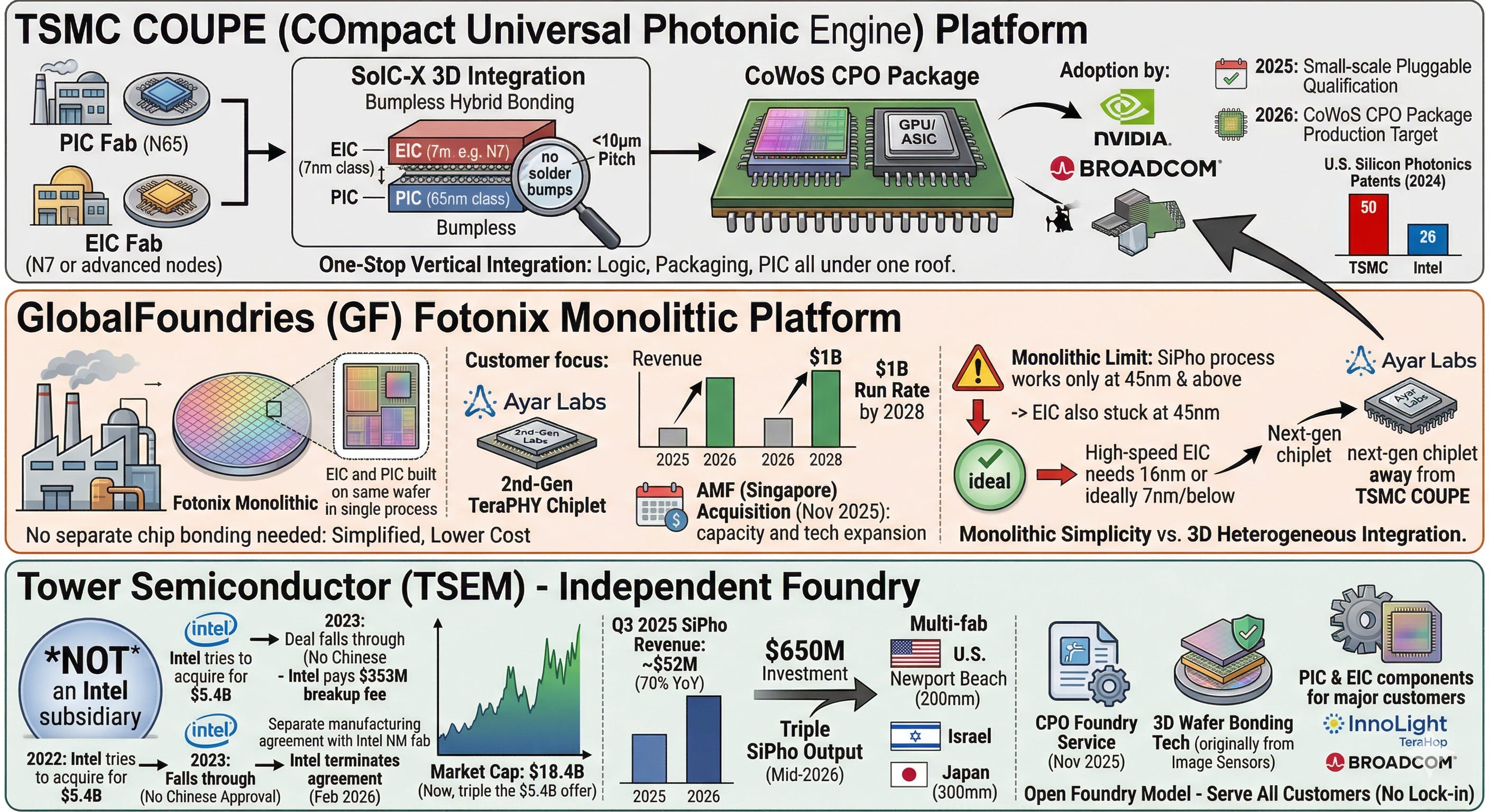
TSMC is the most watched name in the CPO world. They built the COUPE (COmpact Universal Photonic Engine) platform. PICs are fabricated on an N65 process (65nm-class), while EICs (electronic chips) are built on N7 (7nm) or more advanced nodes. The two are then stacked vertically using SoIC-X, TSMC’s 3D integration technology. This is bumpless hybrid bonding, where chip surfaces are joined directly without solder bumps, with bond pitch below 10μm, extremely dense.
Both NVIDIA and Broadcom have adopted COUPE. TSMC completed qualification for small-scale pluggable applications in 2025 and is targeting CoWoS CPO package production in 2026. In 2024, they filed 50 silicon photonics patents in the U.S., nearly double Intel’s 26. A latecomer, but catching up at a frightening pace. TSMC’s advantage is offering advanced logic processes (N7, N5, N3) and advanced packaging (CoWoS, SoIC) under one roof. Make the PIC, make the EIC, integrate them, then put it all together with the GPU or ASIC. One-stop vertical integration that no other foundry can replicate.
GlobalFoundries (GF) claims the world’s largest dedicated SiPho production capacity. Their platform is Fotonix, and it takes a fundamentally different approach from TSMC. Fotonix is monolithic, building the EIC and PIC on the same wafer in a single process. No separate chip bonding needed, which simplifies packaging and lowers cost. Ayar Labs’ second-generation TeraPHY chiplet is manufactured on GF Fotonix. In November 2025, GF acquired AMF (Advanced Micro Foundry), a Singapore-based SiPho specialist fab, expanding both capacity and technology portfolio. Three days ago at their investor day, GF announced that SiPho revenue would double in 2025 and double again in 2026, targeting a $1B run rate by 2028.
However, monolithic has an inherent limitation. The SiPho process only works at 45nm and above, which means the EIC on the same wafer is also stuck at 45nm. High-speed EICs need 16nm at minimum, ideally 7nm or below. Monolithic can’t deliver that. This is exactly why Ayar Labs is moving its next-generation chiplet to TSMC’s COUPE (3D heterogeneous integration). Whether GF can defend its position with monolithic’s simplicity and cost advantages, or whether TSMC’s 3D integration becomes the standard, is one of the defining axes of the foundry competition.
Tower Semiconductor is an Israel-based independent specialty foundry (NASDAQ: TSEM). There’s an important fact here that many people get wrong. A lot of people think Tower is an Intel subsidiary. It is not. Intel tried to acquire Tower for $5.4B in 2022, but the deal fell through in August 2023 when Chinese regulatory approval never came. Intel paid Tower a $353M breakup fee and that was it. There was a subsequent manufacturing agreement for Intel’s New Mexico fab to produce wafers for Tower customers, but in February 2026, Intel notified Tower it would not honor that agreement. Tower stayed independent and is arguably thriving. Its market cap is now $18.4B, more than triple what Intel offered to pay.
Tower’s SiPho business is growing fast. Q3 2025 SiPho revenue alone was about $52M (70% year-over-year growth), targeting $220M+ for full-year 2025. They’re investing $650M to triple SiPho output by mid-2026. They operate SiPho fabs in the U.S. (Newport Beach, 200mm), Israel, and Japan (300mm). In November 2025, they announced a CPO Foundry service, extending their existing 3D wafer bonding technology (originally developed for image sensors) into SiPho and SiGe CPO packaging. They’ve been manufacturing PIC and EIC components for major customers including InnoLight (TeraHop) and Broadcom, and are now extending into CPO. Tower’s strength is its open foundry model, serving all customers without lock-in to any single buyer.
Tower Semiconductor: Everything You Need to Know

Silicon photonics foundry. Still an unfamiliar term for many, but right now it’s one of the hottest keywords in the semiconductor industry. A factory that mass-produces chips that transmit data using light. Tower is currently standing at the front of that line. It is the de facto sole volume supplier of 1.6T (1.6 terabits per second) PICs (Photonic Integrated Circuits), and it serves as the primary foundry for both pluggable transceivers and CPO (Co-Packaged Optics, the next-generation technology that places optical modules inside the chip package).
Scale-up perspective: Putting PICs inside GPU packages demands extremely high performance uniformity. Package costs run from tens of thousands to $100K+, so a single PIC defect scraps the whole thing. TSMC’s 3D integration has an edge here because it enables the highest-performance EICs.
Scale-out perspective: Switch CPO package costs are lower than scale-up, making the economic impact of defects relatively smaller. GF’s monolithic approach and Tower’s cost-efficient model can be competitive in this space.
4-2. EIC-PIC Integration: Three Ways to Combine Two Chips, All with Problems
CPO, Fully Dissected [CPO Special Part 2]
![CPO, Fully Dissected [CPO Special Part 2]](https://substackcdn.com/image/fetch/$s_!LFif!,w_1300,h_650,c_fill,f_webp,q_auto:good,fl_progressive:steep,g_auto/https%3A%2F%2Fsubstack-post-media.s3.amazonaws.com%2Fpublic%2Fimages%2Fd2df124c-d6b0-4142-833c-908be262ab7c_900x491.jpeg)
Part 1 answered the question of why CPO exists. Now we move to the next question. If you crack open a chip package with CPO, what’s actually inside? What does each component do, and how do they all c…
The EIC (electronic chip, signal processing) and PIC (photonic chip, light control) are two distinct chips with different functions. How you combine them completely changes the performance, cost, and thermal profile. (The three approaches were introduced in 4-1 alongside the foundry discussion, but here we go deeper into the strategies of the companies that chose each one.)
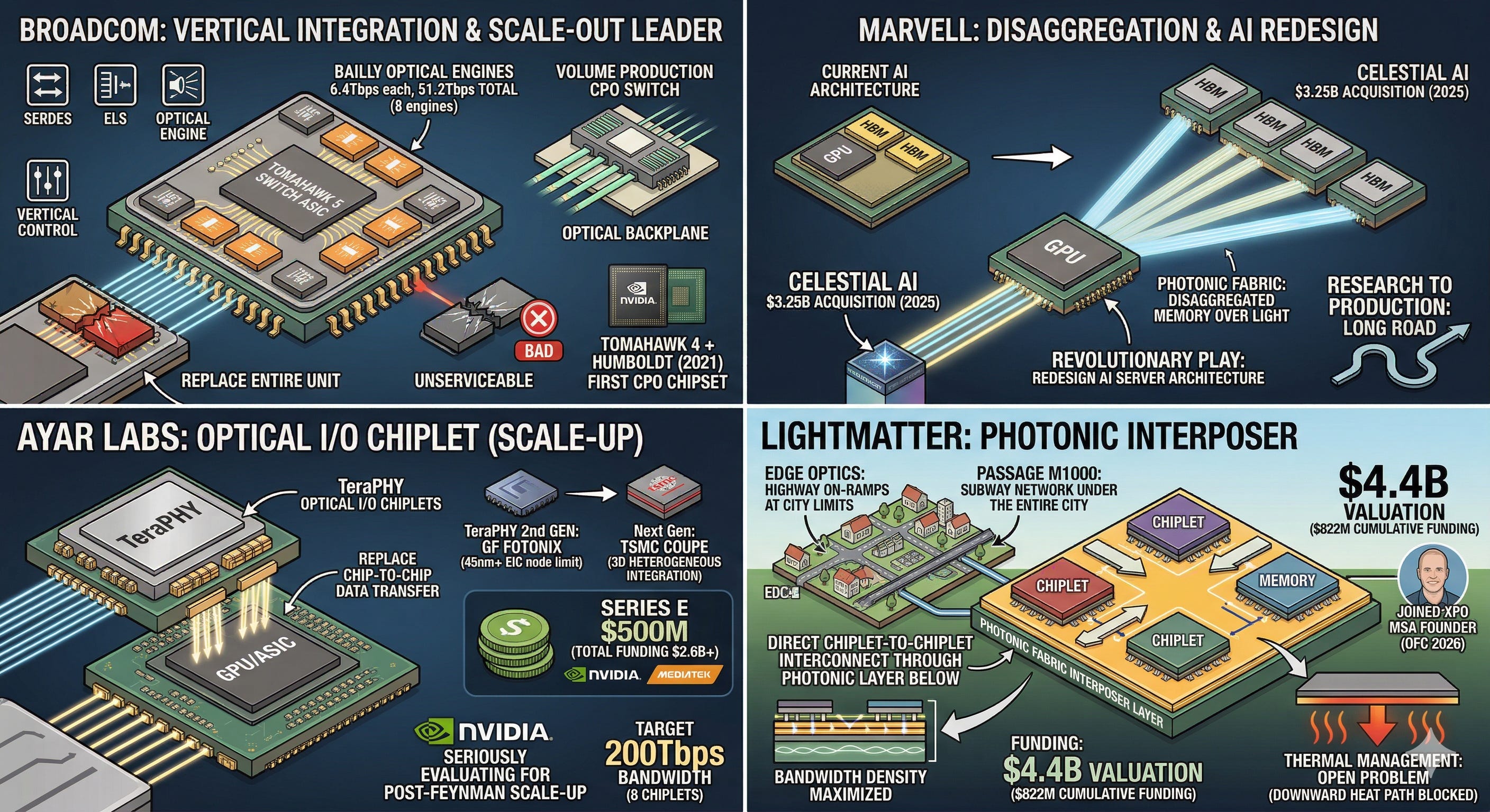
Broadcom leads the CPO ecosystem. In 2021, they created the industry’s first CPO chipset with the Tomahawk 4 plus Humboldt combination. Their second-generation Tomahawk 5 plus Bailly delivered the industry’s first volume production CPO switch. Each Bailly optical engine runs at 6.4Tbps, with 8 engines per switch package reaching 51.2Tbps total. A third-generation 200G-per-lane CPO is already in development. At OFC 2025, they demoed 6.4Tbps optics integration for custom AI accelerators (XPUs). Broadcom’s advantage is vertical integration from the switch ASIC through SerDes, optical engine, and ELS ecosystem. They’re the de facto leader in scale-out CPO. But Bailly’s optical engines are permanently embedded in the package. If one fails, the whole thing gets replaced. This serviceability problem is a real barrier to hyperscaler adoption.
Marvell comes from a different angle. Their own 3D SiPho engine design with 200Gbps electrical/optical interface is competitive, but the game-changer was the $3.25B acquisition of Celestial AI in February 2025. Celestial AI’s Photonic Fabric doesn’t just send data between chips using light. It disaggregates memory from compute over an optical link. In today’s AI architecture, GPUs and HBM physically share the same package. If Photonic Fabric works at scale, HBM could sit in a separate package and connect to the GPU through light. This goes beyond winning the CPO market. It’s a play to redesign AI server architecture itself. That’s why Marvell wrote the $3.25B check. To be clear, this is still closer to research than production, with a long road to commercialization.
Ayar Labs is the key startup in scale-up CPO. They build an optical I/O chiplet called TeraPHY. Drop it into a GPU or ASIC package, and it replaces copper with light for chip-to-chip data transfer. The second-generation TeraPHY was manufactured on GF’s monolithic Fotonix process, but due to the EIC node limitation (stuck at 45nm+) discussed earlier, the next generation is moving to TSMC COUPE (3D heterogeneous integration). Three weeks ago they closed a $500M Series E with NVIDIA and MediaTek participating, pushing cumulative funding past $2.6B. They’re collaborating with GUC (a TSMC subsidiary) and Alchip on reference designs, targeting up to 200Tbps bidirectional bandwidth with 8 TeraPHY chiplets in a single package. The fact that NVIDIA invested directly signals that NVIDIA is seriously evaluating Ayar’s technology for post-Feynman scale-up CPO.
Lightmatter takes the most ambitious approach. While other companies place optical engines at the chip’s edge, Lightmatter builds the Passage M1000, a silicon photonic interposer that lays photonic fabric underneath the chip. An analogy: other companies put highway on-ramps at the city limits, while Lightmatter builds a subway network under the entire city. Chiplet-to-chiplet interconnect doesn’t need to route through the chip edge. It connects directly through the photonic layer below. Bandwidth density can be maximized. They’ve hit a $4.4B valuation with $822M cumulative funding. Interestingly, at OFC 2026, they also joined the XPO MSA as a founding member, straddling both the CPO and pluggable camps. The caveat: verification of actual GPU or ASIC operation on top of a photonic interposer is still early-stage, and thermal management (with photonic fabric below the chip, the heat dissipation path downward gets blocked) remains an open problem.
4-3. Thermal Management: CPO’s Most Fundamental Contradiction
What’s the problem?
Section 2 touched on the thermal challenge. Here we go deeper. CPO’s core value proposition is power savings. But thermal management can eat those savings right back. That’s CPO’s most fundamental contradiction.
Where things stand and how the industry is responding.
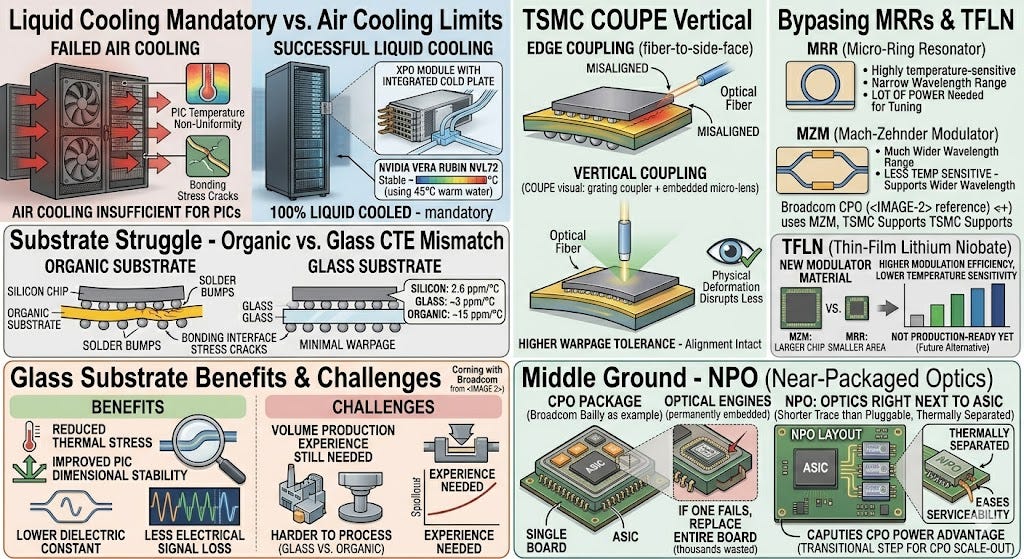
Liquid cooling is mandatory. That’s industry consensus. Air cooling can’t maintain the temperature uniformity PICs require. NVIDIA’s Vera Rubin NVL72 is already 100% liquid cooled (using 45°C warm water), and XPO adopted an integrated cold plate inside each module. Any system that runs CPO will be liquid cooled, no exceptions.
Glass substrate is emerging as a replacement for organic substrate. Today, most semiconductor packages mount chips on organic substrates. The problem is that organic substrate has a CTE (Coefficient of Thermal Expansion) that’s far from silicon’s. When temperature rises, the substrate expands a lot while the chip barely expands, building stress at the bonding interface until cracks form. This problem is worse in CPO because PIC waveguides are extremely sensitive to physical dimension changes.
Corning is working with Broadcom on glass substrate CPO packaging. Glass has a CTE much closer to silicon (glass around 3ppm/°C, silicon around 2.6ppm/°C, organic around 15ppm/°C), so the expansion mismatch between chip and substrate shrinks dramatically under temperature swings. Thermal stress drops, and PIC dimensional stability improves. Glass also has lower dielectric constant, which means less high-frequency electrical signal loss. The catch: glass substrate still lacks volume production experience and is harder to process than organic substrate.
TSMC COUPE’s vertical coupling design is another answer to the thermal problem. Edge coupling (connecting fiber to the chip’s side face) falls out of alignment when the chip warps from heat. COUPE’s vertical coupling (grating coupler plus embedded micro-lens receiving light from above) has higher tolerance for warpage. Physical deformation from heat disrupts optical alignment less.
There are also approaches that bypass MRRs entirely. Mach-Zehnder Modulators (MZM) are less temperature-sensitive than MRRs. They operate across a wider wavelength range and need less thermal tuning power. The tradeoff is larger chip area. Broadcom’s CPO uses MZM, and TSMC supports MZM as well. Meanwhile, Thin-Film Lithium Niobate (TFLN), a newer modulator material, is gaining attention. It offers higher modulation efficiency and lower temperature sensitivity than silicon. It’s not production-ready yet, but it could become a long-term alternative to silicon photonics’ thermal problems.
There’s also a middle-ground approach called NPO (Near-Packaged Optics). Instead of placing the optical engine inside the same package as the ASIC, you put it right next to the ASIC on the same board. Thermally separated, but with a much shorter copper trace than pluggable. It captures some of CPO’s power advantage while easing both the thermal and serviceability problems. NPO could see adoption as a transitional step toward CPO in scale-out.
Can it be solved?
The combination of liquid cooling, glass substrate, and MZM or TFLN modulators makes scale-out CPO’s thermal challenge manageable. Broadcom’s Bailly already running is the proof.
Scale-up CPO (3D integration with GPUs at 90°C+) remains unverified. TSMC COUPE’s 2026 production ramp will be the first real-world thermal test. Yield and reliability data from that ramp will determine whether scale-up CPO is truly viable.
4-4. Laser Source: Why NVIDIA Poured $4B into This
What’s the problem?
Heat forces the laser outside the package (the ELS architecture, covered in Section 2). But ELS itself has problems.
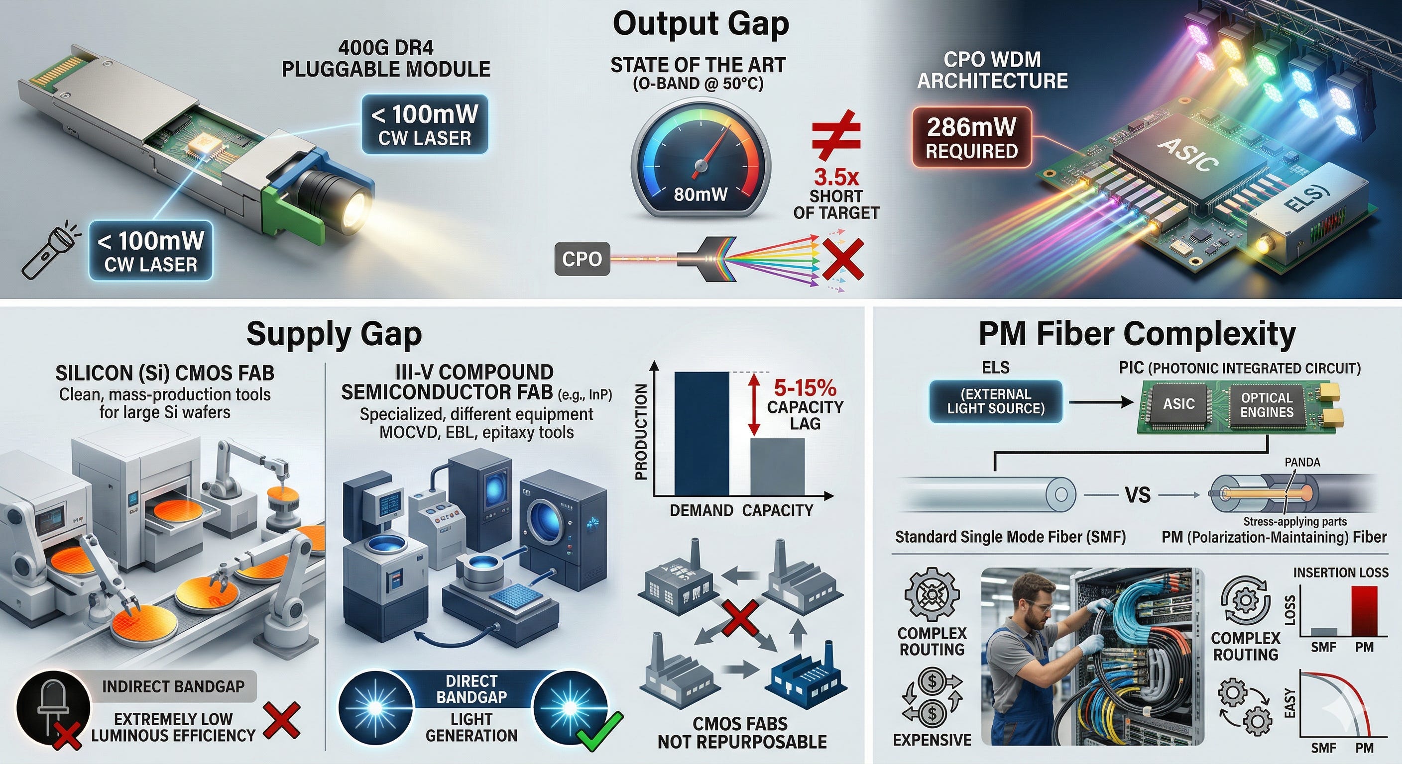
Output gap. A pluggable 400G DR4 module’s CW laser needs less than 100mW of output. Think flashlight. A CPO WDM architecture requires 286mW. A single laser has to feed light into multiple wavelength channels simultaneously. You need stage lighting, not a flashlight. Current state of the art in O-band at 50°C tops out at about 80mW. That’s 3.5x short of the target.
Supply gap. High-power CW laser production capacity lags demand by an estimated 5 to 15%. Lasers are made from III-V compound semiconductors (primarily InP, indium phosphide). Silicon can’t efficiently generate light because it’s an indirect bandgap material with extremely low luminous efficiency. III-V fabs use entirely different equipment and processes from CMOS fabs, so existing factories can’t be repurposed. Purpose-built facilities are required.
PM fiber complexity. Delivering light from the ELS to the PIC requires maintaining polarization, which means PM fiber. PM fiber is expensive, routing is complex, and it adds insertion loss.
How the industry is responding.
What NVIDIA did three weeks ago is the most direct answer. They signed simultaneous multi-year supply contracts with Coherent (formerly II-VI) and Lumentum, $2B each, $4B total. Coherent is the global number one in III-V lasers. Lumentum is the other titan. Committing $4B to both at once reflects the calculation that relying on a single source carries unacceptable supply risk. If this $4B goes toward laser fab expansion, the capacity gap could narrow meaningfully by 2027 to 2028.
Multi-wavelength lasers are another path forward. Today, WDM requires a separate laser for each wavelength. Four wavelengths means four lasers. Scintil Photonics (France) is developing epitaxial III-V on silicon technology that integrates multiple laser wavelengths on a single chip. If it works, the number of lasers drops dramatically. Cost, complexity, and fiber routing all simplify.
NVIDIA’s detachable OSA (Optical Sub-Assembly) addresses the serviceability side of the laser problem. In Quantum-X CPO, they designed the module containing the optical engine to be removable. The ELS itself was always pluggable and easy to swap, but NVIDIA went a step further and made the optical engine itself field-replaceable. A direct contrast to Broadcom’s Bailly, where the optics are permanently embedded.
Worth noting: Coherent and Lumentum currently generate a significant share of their revenue from pluggable transceiver components. When CPO scales, pluggable component revenue declines, but ELS component revenue rises. These companies aren’t CPO “victims.” They’re transitioners.
Can it be solved? The output gap (80mW vs. 286mW) is an engineering challenge, not a fundamental physical limit. High-power O-band CW laser development is underway, and NVIDIA’s $4B investment accelerates the timeline. By 2027 to 2028, both output and capacity gaps should narrow significantly. Not fully closed, but enough to support initial CPO deployments.
4-5. Test and Known Good Die: Minutes Per Die, and That’s the Problem
What’s the problem?
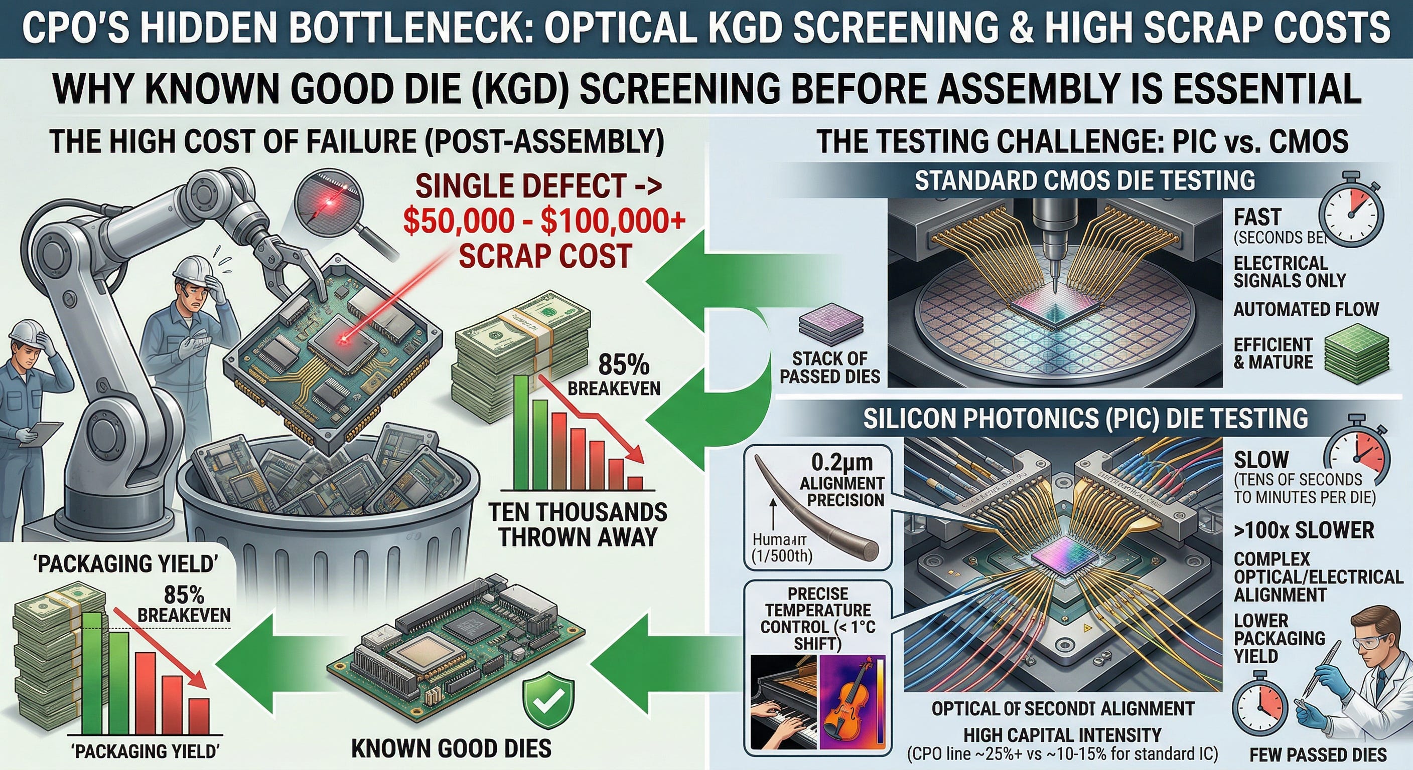
The most underestimated bottleneck in CPO. “One defect after assembly means scrapping the entire package.” Tens of thousands to $100K+, thrown away whole. That’s why KGD (Known Good Die) screening before assembly is essential. The problem: testing silicon photonics die is fundamentally hard.
Think about how normal chip testing works. A probe card’s metal pins touch the chip’s electrical pads, inject electrical signals, read the response. Done in seconds per die.
PICs can’t be tested that way. You have to inject light and read light back. The probe card needs both electrical pins and optical fiber attached simultaneously. Left hand on the piano, right hand on the violin. That fiber has to be aligned to the waveguide within 0.2μm (1/500th of a human hair). Temperature has to be precisely controlled too (behavior shifts with 1°C). The result? Tens of seconds to several minutes per die. Over 100x slower than CMOS.
Most of the work today is still manual. No automated production flow has been established. Packaging yield can’t break past the 85% breakeven mark, and CPO line capital intensity jumps from 10 to 15% for standard IC packaging to 25% or higher.
How the industry is responding.
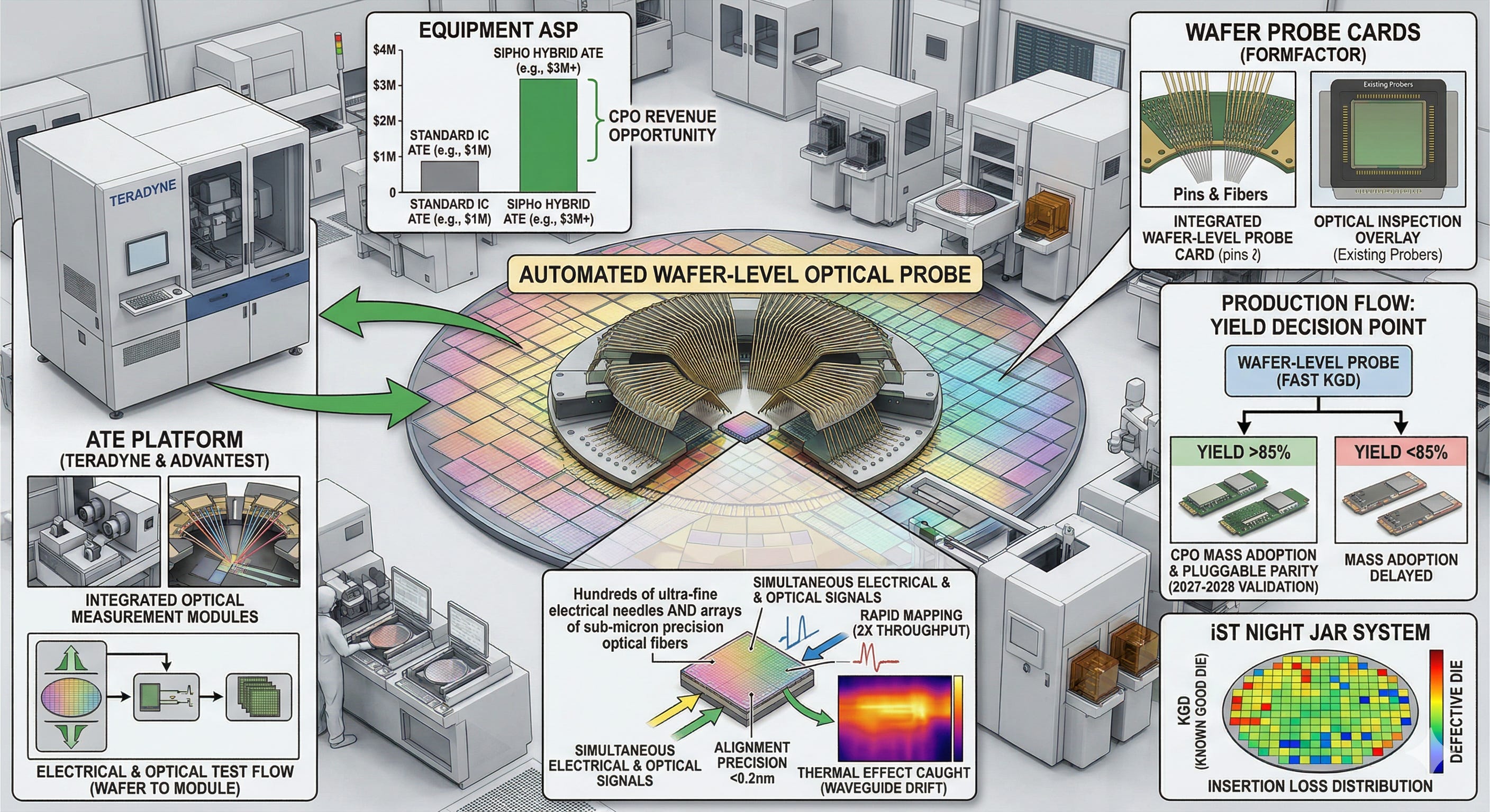
The key is wafer-level optical test automation. If you can test die automatically and quickly while they’re still on the wafer, instead of probing them one by one by hand, that’s the game changer.
Teradyne (number one in ATE) is the most aggressive. They’re developing a CPO hybrid test solution that integrates optical measurement modules into their existing ATE platform. The goal: electrical and optical testing, simultaneously, automatically, at the wafer level. Advantest (number two in ATE) is also ramping investment in photonics test capability.
FormFactor approaches it from the probe card side. They’re developing wafer-level probe cards with both electrical pins and optical fiber attached simultaneously. If this works, you can add optical inspection on top of existing wafer prober infrastructure.
Taiwan’s iST partnered with Enlitech to build a verification platform covering wafer-to-module stages for SiPho die. Their Night Jar system rapidly maps insertion loss distributions and catches waveguide drift and modulator instability caused by thermal effects at the wafer level. According to the company, throughput is more than 2x the current mainstream optical tools, with alignment precision of 0.2nm.
For equipment companies, this is an opportunity. SiPho testing is more complex and more expensive than standard digital chip testing. Equipment ASPs go up. For ATE players like Teradyne and Advantest, CPO delivers two opportunities at once: a new market and higher ASPs.
Can it be solved? Wafer-level optical test automation is in development, not finished. At current capability, breaking past 85% packaging yield is difficult. The first production-scale validation of automated test flows is expected around 2027 to 2028. If yield clears 85% at that point, CPO unit economics approach parity with pluggable. If it doesn’t, mass adoption gets pushed further out. Testing is quiet, but it’s CPO’s most decisive gatekeeper.
Scale-up perspective: Packages at $100K+. The financial impact of failed KGD screening is maximum. Test precision requirements are the highest.
Scale-out perspective: Per-die financial impact is smaller, but volume is much larger. Manual testing can’t handle the throughput. Test automation is the gatekeeper for scale-out CPO mass production.

4-6. Fiber Coupling: Connecting a 9μm Pipe to a 0.5μm Channel
What’s the problem?
PIC waveguide core: roughly 0.5μm by 0.2μm. Single-mode fiber core diameter: 9μm. The light mode sizes differ by about 20x. Like trying to push water from a garden hose (fiber) into a hypodermic needle (waveguide). Just point one at the other and most of the light fails to couple and scatters away. A mode-size converter is essential, and even after that, alignment tolerance is 0.2μm.
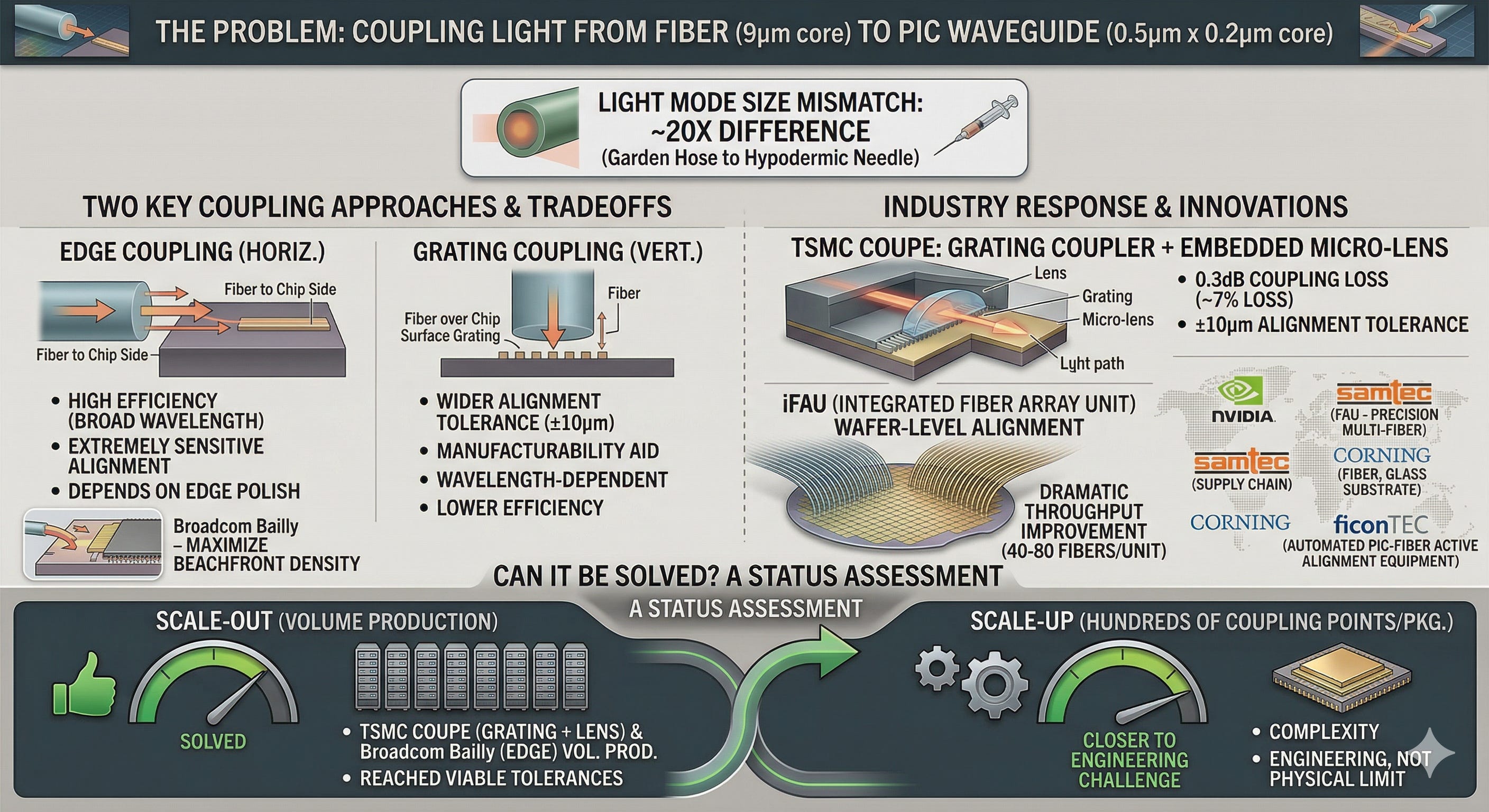
Two approaches and their tradeoffs.
Edge coupling connects the fiber horizontally to the chip’s side face. High efficiency across a broad wavelength range, but extremely sensitive to mechanical alignment. Depends on chip edge polishing quality. Broadcom’s Bailly uses this approach to maximize beachfront density.
Grating coupling etches a fine grating pattern on the chip surface and receives light vertically. Alignment tolerance is much wider (±10μm), which helps manufacturability. But it’s wavelength-dependent, and coupling efficiency can be lower than edge coupling.
How the industry is responding.
TSMC COUPE adopted a grating coupler plus embedded micro-lens combination. Micro-lenses formed inside the chip focus the light while increasing tolerance against chip warpage. According to TSMC’s published data, this achieves 0.3dB coupling loss with ±10μm alignment tolerance. 0.3dB means only about 7% of light is lost. They’re also developing an iFAU (integrated Fiber Array Unit) process that aligns 40 to 80 fibers in rows at the wafer level. If wafer-level fiber alignment works, throughput improves dramatically compared to attaching fiber to each die individually.
Samtec plays a critical role in NVIDIA’s CPO supply chain, supplying FAUs (Fiber Array Units), precision-arrayed multi-fiber assemblies that connect to each optical engine. Corning makes the optical fiber, PM fiber, and glass substrates. Germany’s ficonTEC leads the effort to automate PIC-fiber active alignment, replacing today’s manual fiber alignment with automated production equipment.
Can it be solved? Fiber coupling is the closest to solved among CPO’s bottlenecks. TSMC COUPE’s vertical coupling plus micro-lens combination has reached production-viable tolerance levels, and Broadcom Bailly’s edge coupling is already working in volume production. For scale-out, consider it solved. Scale-up still has the complexity of hundreds of fiber alignment points per package, but that’s closer to an engineering challenge than a fundamental physical limit.
5. When CPO Fully Arrives, Does Pluggable Disappear?
Short answer: no.
First, CPO can’t cover every use case. CPO is optimized for high-density, high-bandwidth links like switch-to-switch and GPU-to-GPU. Data centers also have server-to-switch uplinks, management networks, DCI (data center interconnect), and other link types. These need lower per-port bandwidth and prioritize flexibility and compatibility. That stays pluggable territory.
Second, serviceability always matters somewhere. The operational convenience of pulling a failed module and plugging in a new one can’t be replaced. In enterprise data centers, colocation facilities, and telco networks that aren’t hyperscaler operations, pluggable remains the standard.
Third, pluggable itself keeps evolving. LPO cuts power. XPO boosts density. Coherent ZR/ZR+ pluggables own the DCI market. CPO has no reason to enter that space.
The expected outcome is coexistence. CPO takes the high-density scale-up and high-end scale-out segments. Pluggable keeps everything else. EUV dominates leading-edge nodes, but DUV still sells perfectly well at mature nodes. Same dynamic.
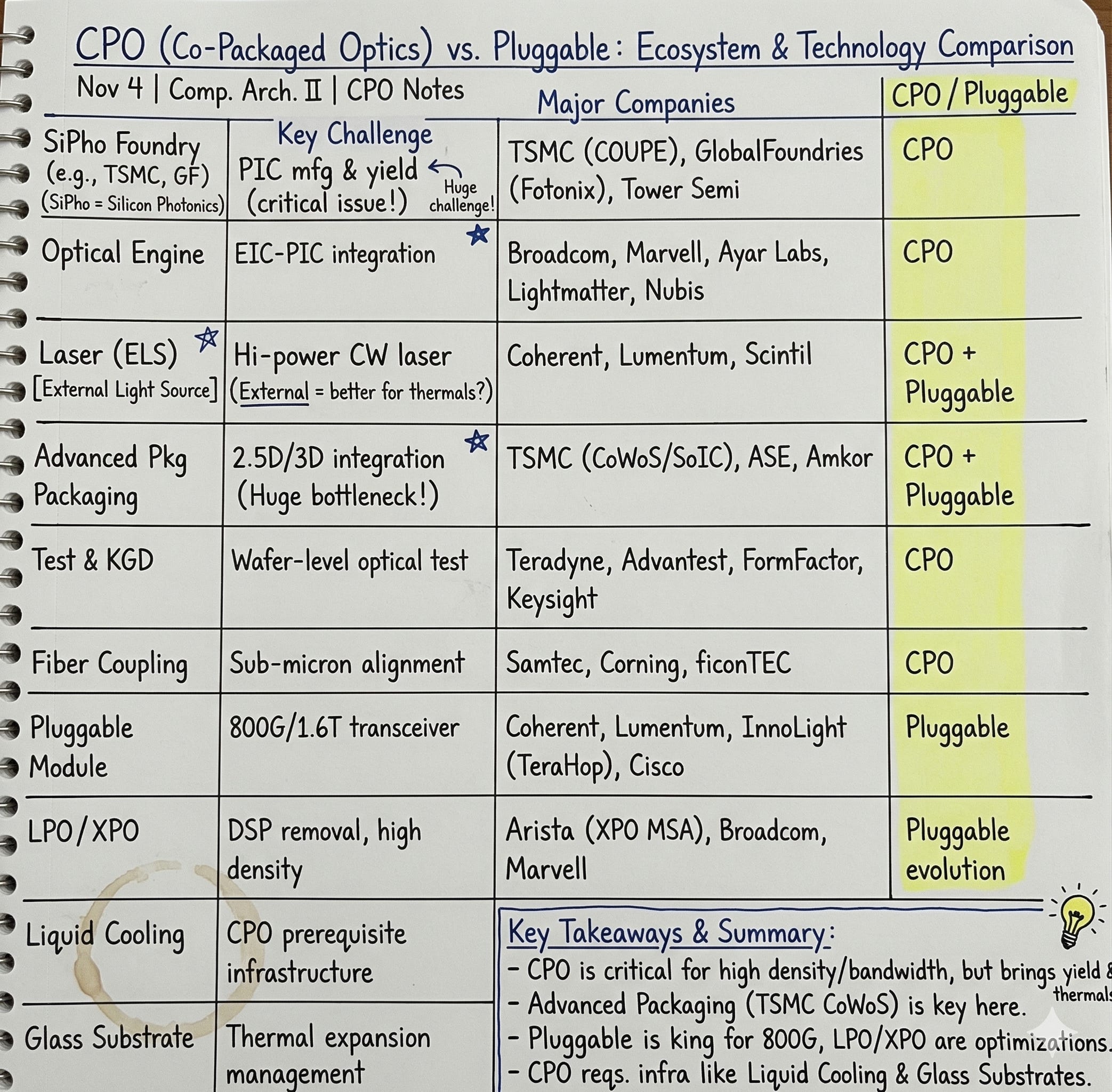
6. Company Mapping by Technology Area
7. What Investors Should Watch: Monetization Timeline and Leading Indicators
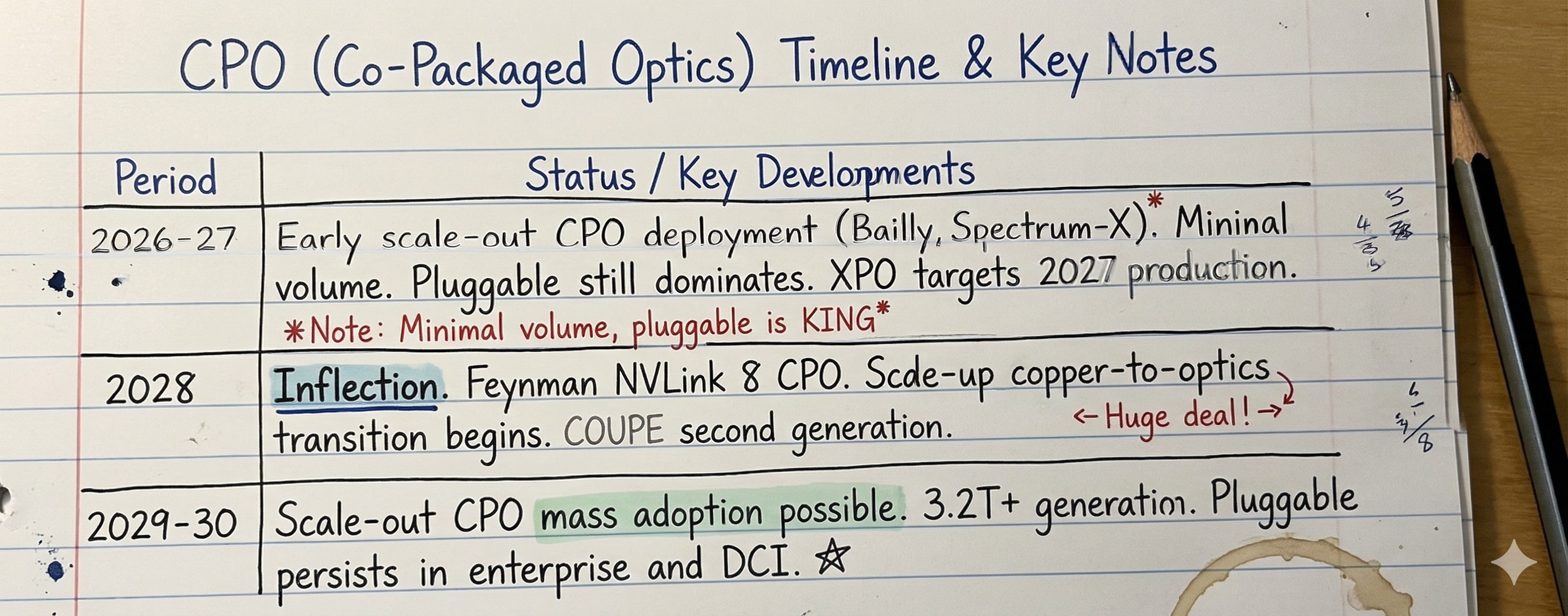
Timeline
Five Leading Indicators
① NVIDIA CPO switch real deployment volumes. Jensen said “full production.” Production and deployment are different things. Track whether Lambda, CoreWeave, and TACC actually receive hundreds of units or more.
② Hyperscaler official CPO commitments. A large-scale adoption announcement from Microsoft, Google, Meta, or Amazon would be the tipping point. As of now, Microsoft backs XPO MSA (the pluggable side).
③ Coherent/Lumentum revenue mix. A decline in pluggable revenue signals CPO transition. A rise in ELS revenue signals supply chain activation. Track both numbers together.
④ TSMC COUPE yield disclosure. Whether 300mm wafer insertion loss uniformity reaches production grade. No public data means production isn’t ready.
⑤ GF vs. TSMC SiPho competitive dynamics. Ayar Labs and Broadcom have adopted COUPE. But GF announced its $1B run rate target just three days ago. Both sides are investable. Watch whether TSMC becomes the de facto standard or GF defends its niche with monolithic.
Beneficiary Framework
Near-term (2026-27): Pluggable demand explodes because CPO isn’t ready yet. 800G/1.6T transceivers (Coherent, Lumentum, InnoLight). Advanced packaging (TSMC, ASE, Amkor).
Medium-term (2028-30): TSMC COUPE becomes the key platform. Coherent/Lumentum transition to ELS. Test equipment (Teradyne, Advantest) ASP uplift. GF SiPho grows.
High-risk/High-reward: Ayar Labs (pre-revenue, possible IPO), Lightmatter (validation still early).
Closing: Conviction Comes from Coordinates, Not Direction
The direction is right. Copper is hitting physical limits, and the shift to optical is a matter of when, not if. Jensen knows it. Hock Tan knows it. Everyone knows it.
But the direction being right and the timing being right are two different things. Today, CPO shipment volume is zero. Pluggable ships 50 million units. The $4.5B being invested is a bet on 2028 and beyond, not 2026 reality.
Scale-up CPO replaces copper, starting with Feynman in 2028. Scale-out CPO has started, but isn’t decisively beating pluggable. Pluggable doesn’t die. It evolves with LPO and XPO, staying alive in every space CPO can’t reach.
Plenty of investors know the direction. Very few know the current coordinates. Same direction, different coordinates, different entry points. Different entry points, different returns. A position built on knowing the coordinates can survive when the market shakes. And investors who can hold through the shaking are the ones who win.
Disclaimer
This content is not investment advice and does not recommend buying, selling, or holding any security. All investment decisions and responsibility remain solely with the investor.
Hi Damnang, appreciate your great in-depth analysis. My question is if eliminating DSP can save 10W per module, and if we assume 144 DSPs per rack of GB200 NVL72 which consumes 120-130kW, it's only 1% of the total power consumption? Isn't it so small to make power saving a compelling case for cpo adoption?
매우 잘 읽었습니다. 좋은 글 감사합니다.