

Optics has been one of the hottest themes in AI infrastructure investing over the past year. Shares of optical component and module companies have multiplied, and CPO has drawn attention right in the middle of that move.
By now, most investors have at least heard the term co-packaged optics.
But does the market really know CPO?
Ask which components come from where, what path they travel before ending up inside a switch, and which companies along that path are bottlenecks versus bystanders, and suddenly very few people have answers.
The early production ramp is starting now, and this is the point where that difference starts showing up in returns. Preparing for the second phase of the optics trade means knowing the supply chain behind the name.
This article follows that supply chain to the end.
Where the light is made, who fabricates the chips that load signal onto it, where the two meet to become a single switch, and who inspects every seam along the way.
I first draw a map of the entire CPO supply chain from materials to systems, then layer on the field accounts and the industry's felt temperature that filings and IR decks alone cannot show.
On top of that come six CPO investment theses, and finally the investment strategy grounded in those Theses, all of it covered here.
Read this to the end and I am confident you will see what comes next in optics investing.
Table of Contents
The CPO Supply Chain Map: From Materials to Systems
Voices from the Field: What Is Actually Circulating Around CPO in 1H 2026
When CPO Really Arrives: Six Theses and the P&L Arithmetic by Layer
From Thesis to Position: Core, Satellites, and Options
Closing: The Thesis Verification Calendar
Disclaimer
This article is for informational purposes only and is not a recommendation to buy or sell any security. The unit prices, multiples, and ratios used in the arithmetic below are the author’s scenario inputs, not disclosed data, and are meant to show direction and magnitude rather than precise forecasts. Prices and valuations are as of the time of writing and may have changed since. The stock arrangement is derived from the thesis structure in this article; names not included here may well outperform, and responsibility for investment decisions and their outcomes rests with the investor.
1. The CPO Supply Chain Map: From Materials to Systems
Behind every CPO switch, two manufacturing chains with different starting points run in parallel: the chain that makes the light itself, and the chain that loads signal onto that light.
CPO, Fully Dissected [CPO Special Part 2]
![CPO, Fully Dissected [CPO Special Part 2]](https://substackcdn.com/image/fetch/$s_!LFif!,w_1300,h_650,c_fill,f_webp,q_auto:good,fl_progressive:steep,g_auto/https%3A%2F%2Fsubstack-post-media.s3.amazonaws.com%2Fpublic%2Fimages%2Fd2df124c-d6b0-4142-833c-908be262ab7c_900x491.jpeg)
Part 1 answered the question of why CPO exists. Now we move to the next question. If you crack open a chip package with CPO, what’s actually inside? What does each component do, and how do they all connect? And once you’ve solved the problem for switches, where does the technology go from there?
The chain of light starts from a single-crystal InP boule, an ingot in industry terms. Unlike silicon, InP is a direct bandgap material that can convert current into light, so on substrates sliced from the ingot, MOCVD equipment stacks quantum wells one atomic layer at a time, and the result is processed into DFB laser dies.
Lasers for CPO are high-power CW parts at 400mW and above, 6 to 11 times stronger than the CW lasers in existing SiPho transceivers (30 to 70mW). The laser only makes the light and hands modulation to the engine inside the package, but in exchange it has to deliver enough output to survive the coupling and splitting losses on the way to the engine, while still meeting noise specs like linewidth and RIN.
The War of Light, A Laser Shortage

On March 2, 2026, NVIDIA invested $2B in Coherent and another $2B in Lumentum. Both companies make lasers. The two announcements came on the same day and included “multi-billion dollar purchase commitments” and “future capacity access rights.” Jensen Huang wasn’t just buying lasers. He was locking up the ability to make them.
Assemble this laser into a module, complete optical alignment and burn-in, and you have an ELS, an external laser source. The reason the laser lives outside the package is heat. The neighborhood next to a switch ASIC is too hot for a laser to survive.
The chain of signal starts from an SOI wafer. An oxide layer has to be buried beneath the silicon layer to confine light inside a waveguide. This wafer becomes a photonic IC at a PIC foundry, etched with waveguides and modulators, and once the EIC built on a separate CMOS process is mounted on top via hybrid bonding, you have an optical engine. The two chains meet for the first time at packaging.
The engines mount onto the same package substrate around the switch ASIC at the center, light from the ELS is injected through polarization-maintaining fiber, and light carrying signal exits through detachable connectors to the front panel. Past chassis integration and system test, a switch is complete.

What deserves attention is the seams between the processes. Light converts misalignment at the micron level directly into loss, which is why an inspection and test gate sits at every seam. Divide the chain along these seams and the skeleton of the map emerges:
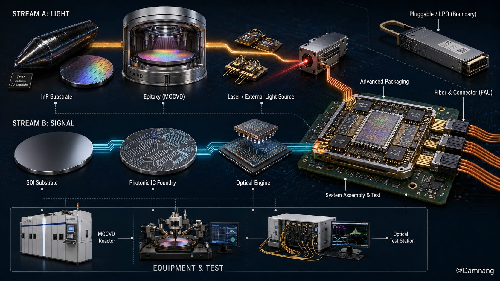
Stream A, the chain that makes light, with three layers;
Stream B, the chain that handles signal, with three layers;
the convergence point where the two streams meet, with three layers;
two horizontal axes of equipment and test cutting across the entire chain;
and the boundary camp outside CPO that shakes the pace of penetration.
The platform is the demand variable that determines attach rate, meaning how many out of every 100 newly deployed switch ports get built as CPO instead of pluggable, and the revenue of every layer below is indexed to this single variable. Right now that number starts below single digits.
The investment judgments that combine this map with what the field is saying come in the second half of the article.
Stream A: The Chain That Makes Light
A1. InP Substrates
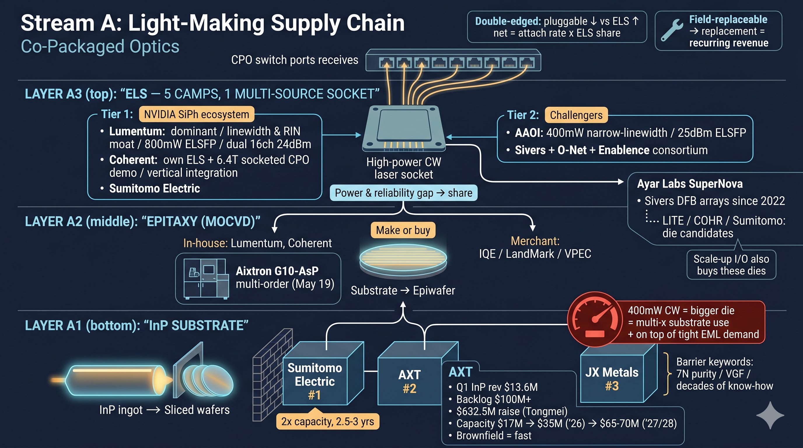
The InP substrate market is an oligopoly with Sumitomo Electric first, AXT second, and the JX Metals family behind them. Growing 7N-purity material into ingots is itself the barrier to entry, and proprietary growth methods like AXT’s VGF represent know-how accumulated over decades. This is not a market a new entrant can break into on a short timeline.
Demand at this layer started printing in the numbers in 2026. AXT’s Q1 InP revenue came in at $13.6M, more than half of total company revenue, and the InP backlog crossed $100M.
In April the company completed a $632.5M raise to fund InP capacity expansion at its subsidiary Tongmei, and kicked off a buildout that doubles InP capacity in 2026 and doubles it again in 2027. On a quarterly capacity basis, the path runs from the historical peak of $17M to $35M by the end of 2026 and $65 to 70M by late 2027 to early 2028.
Competitors are moving too. Sumitomo has also announced a capacity doubling, but guided the timeline at two and a half to three years, while AXT argues it is faster because its expansion is brownfield, converting GaAs lines to InP.
A 400mW-class CW laser has a long cavity, which means a large die, and substrate consumption per laser grows by multiples versus before. That demand is now stacking onto a market that was already tight on existing EML demand even before the CPO ramp.
A2. Epitaxy
The epiwafer is the intermediate good between substrate and laser. Crystal layers have to be grown on the InP substrate via MOCVD before it becomes an epiwafer that can be processed into lasers.
Lumentum and Coherent have this step in house, and those without internal capacity buy from pure-play epi houses like IQE or epi foundries like LandMark and VPEC. Whether a laser maker grows its own epi or outsources it is the fork that splits supply and demand at this layer, and the May 19 disclosure that Lumentum placed multiple orders for Aixtron’s G10-AsP MOCVD is the first public signal that the in-house camp’s expansion has begun in earnest.
A3. Lasers (ELS): A Five-Way Socket Race
High-power CW lasers are currently a market Lumentum dominates. Meeting linewidth and RIN specs at high output is a different order of difficulty from conventional low-power CW, and that technology gap is Lumentum’s moat.
At OFC 2026, Lumentum raised the bar on the output race once more, demonstrating an ELSFP module carrying an 800mW laser and a dual ELSFP coupling 24dBm into fiber via 16-channel multiplexing.
But the camps eyeing this socket have grown to five. The ELS supply chain is forming around the three names publicly listed in NVIDIA’s silicon photonics ecosystem, Lumentum, Sumitomo Electric, and Coherent. On top of that, AAOI followed its December 2025 400mW narrow-linewidth laser with a 25dBm-class ELSFP at OFC, and Sivers threw its hat in with an ELS module announced as a consortium with O-Net and Enablence.
Among the original three, Coherent went as far as a vertical integration move at OFC, demonstrating 6.4T socketed CPO with its own ELS module carrying its own high-power InP CW laser.
On the private side, Ayar Labs’ SuperNova light source has taken Sivers’ DFB laser arrays since 2022, and ahead of the volume ramp, Lumentum, Coherent, and Sumitomo are all mentioned as laser die sources.
Whichever combination wins, the structure is the same: even the scale-up optical I/O camp ends up buying dies from this layer. Given that ELS was designed from the start as a multi-sourced socket, what matters at this layer is not monopoly premium but the technology gap in output and reliability, and that gap eventually converts into share.
For Coherent and Lumentum, CPO cuts both ways. Every port that goes CPO removes pluggable transceiver demand, and the same port creates new ELS demand. The net effect is a function of attach rate and each company’s ELS share.
One more structural point worth noting: ELS is designed to be field-replaceable. A design you swap in the field assumes the reality that lasers are parts that eventually wear out, and at the same time it means replacement demand, a recurring revenue stream, accrues as the installed base grows.
Stream B: The Chain That Handles Signal
B1. SOI Wafers
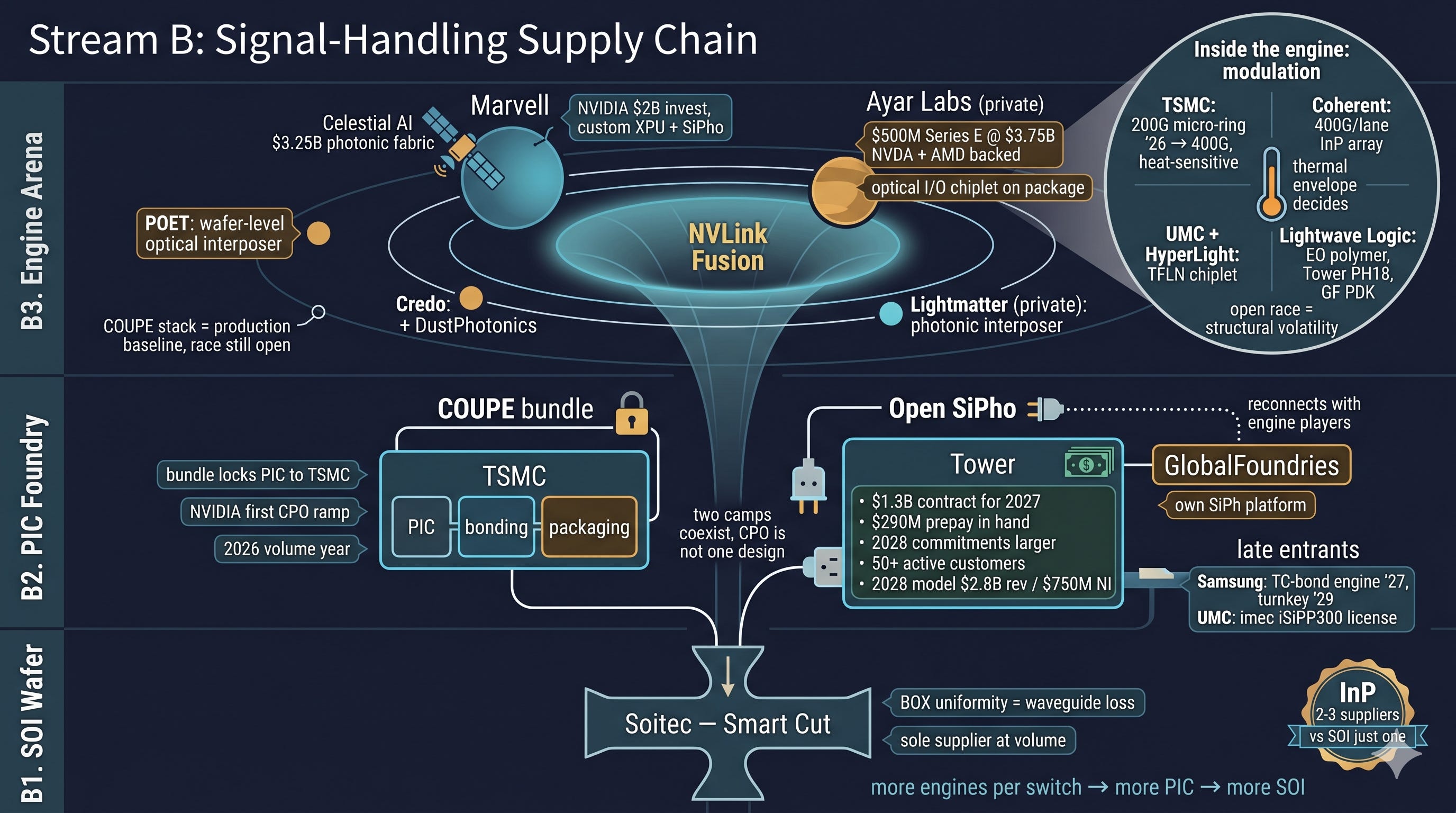
SOI for photonics is a market locked up by Soitec’s Smart Cut. Optical loss in a waveguide is directly tied to the uniformity of the BOX layer and the quality of the silicon layer, and the suppliers who can hit that spec at production scale effectively collapse to Soitec. If InP is an oligopoly of two or three suppliers, this is a bottleneck one notch narrower, effectively down to one. As the number of optical engines per switch grows, PIC demand grows, and PIC demand maps onto SOI shipments.
B2. PIC Foundries
The PIC foundry landscape is a contest among Tower, TSMC, and GlobalFoundries, and the general view is that Tower leads in specialty process depth. And in May 2026, a signal arrived in hard numbers that open SiPho demand is being locked in with real customer money.
Tower disclosed that it signed contracts with its largest customers for $1.3B of SiPho revenue in 2027 and has already received $290M in capacity reservation prepayments. The 2028 volume commitments are larger still, with additional prepayments due by January 2027. Active SiPho customers exceed 50, and the company presented this as the foundation of a 2028 model of $2.8B in revenue and $750M in net income. A foundry contract that extracts prepayments is evidence that the quality of demand is different.
TSMC holds a device that twists the structure. The published COUPE flow is a vertical stack bundling TSMC’s PIC, bonding, and packaging, so a design using COUPE effectively fabricates its PIC at TSMC as well. As long as NVIDIA’s first CPO ramp runs on COUPE this bundle works, and TSMC has nailed down 2026 as the year of COUPE volume production.
But as Tower’s $1.3B contract shows, demand outside the COUPE bundle is plenty large. It means the CPO market is not converging on a single design from NVIDIA alone, and PIC foundries are heading toward a structure where the COUPE-bundle camp and the open camp (Tower, GlobalFoundries) coexist. GlobalFoundries stands in the open camp with its own SiPh platform, and that platform reconnects with several names later in this article.
The latecomers are lining up too. At OFC 2026 Samsung unveiled a roadmap of thermo-compression bonding based optical engines in 2027 and turnkey CPO services in 2029, and UMC made its entry official by licensing imec’s iSiPP300 platform.
B3. Optical Engine Integration and Modulation Technology
Engine integration is the layer with the loudest camp warfare on this map. The COUPE stack is the benchmark in production track record, but the architecture race is not closed, and in 2026 the board actually got bigger.
Marvell closed its acquisition of Celestial AI and its photonic fabric in early February (initial consideration $3.25B), internalizing scale-up optical interconnect capability, and at the end of March took a $2B investment from NVIDIA and joined the NVLink Fusion ecosystem, becoming the camp that connects custom XPUs to SiPho. POET takes a different path with its wafer-level optical interposer, and Credo secured SiPho engine capability through its DustPhotonics acquisition.
On the private side, Ayar Labs is moving fastest. In March it closed a $500M Series E at a $3.75B valuation with NVIDIA and AMD participating, and on June 3 it announced it joined the NVLink Fusion ecosystem.
The scale-up path of attaching optical I/O chiplets directly to compute packages has come under the umbrella of the NVIDIA platform. Celestial AI, once grouped with it among the private big three, has been absorbed into Marvell, and Lightmatter remains with its photonic interposer. The technology paths for scale-up CPO are rapidly aligning around the major platforms.
Inside the engine, a separate race over modulation technology is underway. TSMC published a roadmap for 2026 production of COUPE-based 200G micro-ring modulators with extension to 400G, Coherent demonstrated 400G/lane InP modulator arrays, UMC is pushing TFLN chiplet production with HyperLight, and in the EO polymer camp, Lightwave Logic won a definitive agreement on Tower’s PH18 process in March and got onto GlobalFoundries’ design kit, laying down a foundry track.
Micro-rings are small but temperature sensitive, and TFLN and polymer still have to prove volume production against their performance advantages. The modulation choice ultimately gets decided inside the package’s thermal environment, and until this race closes, volatility at the engine layer is structural.
The Convergence Point: From Package to System
C1. Packaging/OSAT
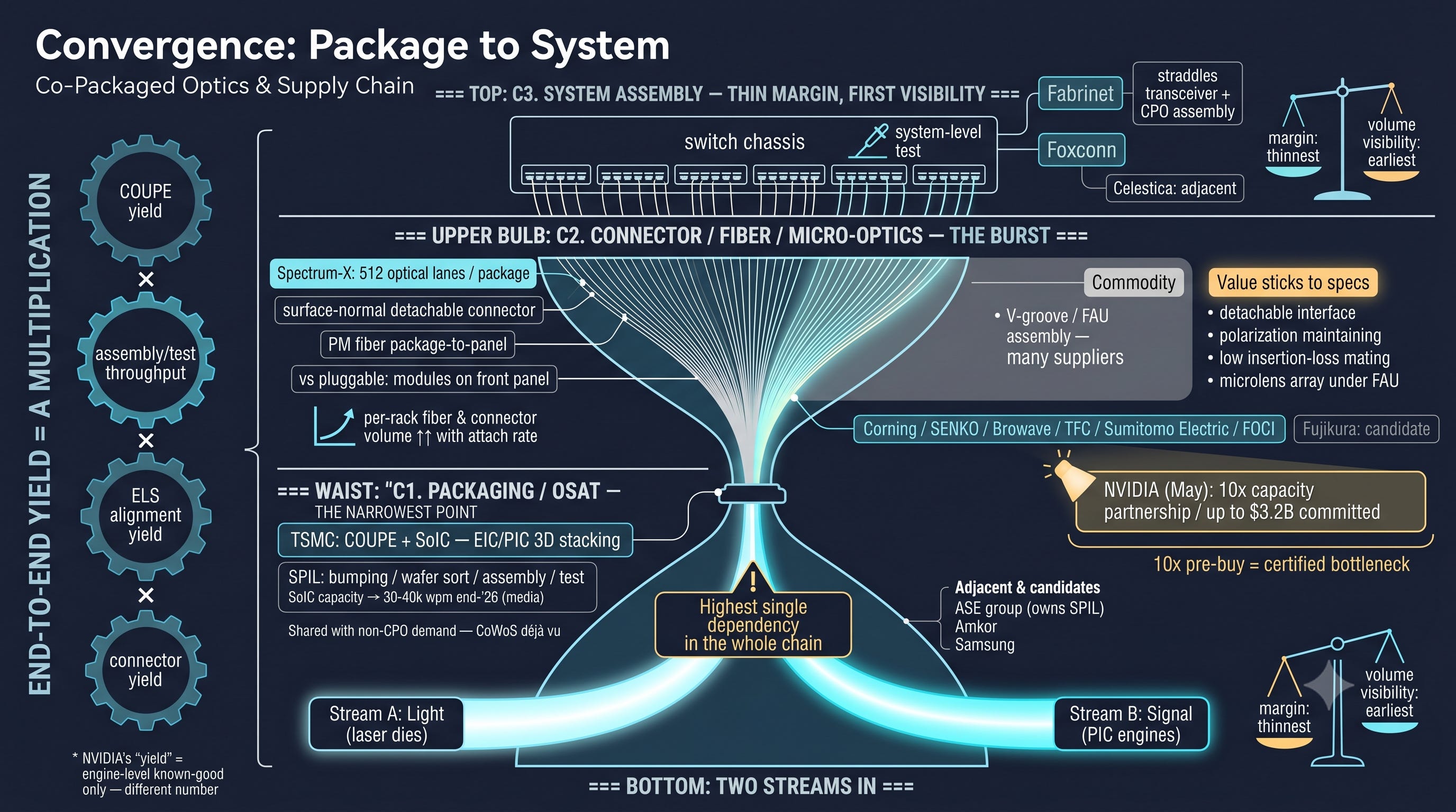
At the packaging stage where the two streams converge, 3D stacking of EIC and PIC is handled by TSMC’s COUPE and SoIC, while bumping, wafer sort, assembly, and test of the multi-chip module are reportedly handled by SPIL. This is the point of highest single-vendor dependence in the entire supply chain.
Lasers are spread across five camps and connectors across even more, but 3D stacking is effectively one. Taiwanese media report TSMC’s SoIC monthly capacity heading toward 30,000 to 40,000 wafers by the end of 2026, and this capacity is shared between CPO and other demand, just as CoWoS was in the HBM era. ASE Group, which owns SPIL, sits adjacent, and Amkor and Samsung are the candidate camps.
The yield assurance NVIDIA emphasizes is an engine-level story, screening for known-good status before engines are attached. End-to-end yield, the product of COUPE yield, assembly and test throughput, ELS alignment yield, and connector yield, is a separate number.
C2. Connectors/Fiber/Micro-Optics
Spectrum-X Ethernet Photonics integrates 512 lanes of optical I/O in a single package and extracts the light through surface-normal detachable connectors. Where pluggables bundled channels by module and plugged into the front panel, CPO lays a dense run of PM fiber and connector assemblies from package to front panel. Fiber and connector content per rack grows with acceleration as attach rate rises.
This layer has to be dissected. V-groove machining and FAU assembly themselves have many suppliers and sit close to commodity. The value concentrates where specs attach: detachable interfaces, polarization maintenance, low insertion loss mating, and sub-layers like the microlens arrays beneath the FAU.
Suppliers are spread across Corning, SENKO, Browave, TFC, Sumitomo Electric, and FOCI, with Fujikura a candidate. In May, NVIDIA signed a partnership with Corning to expand optical connectivity capacity tenfold, with cumulative investment commitments reported at up to $3.2B. A component whose capacity a platform owner pre-secures at 10x is a component certified as a bottleneck candidate.
C3. System Assembly
Integrating the switch and CPO assembly into a chassis and running system-level test falls to Fabrinet and Foxconn, with Celestica an adjacent candidate. Assembly is the thinnest-margin layer in the supply chain, but in exchange it is where volume visibility shows up first. Fabrinet straddles both transceiver assembly and CPO assembly.
The Horizontal Axes: Two Lines That Cut Across the Whole Chain
Axis 1. Equipment
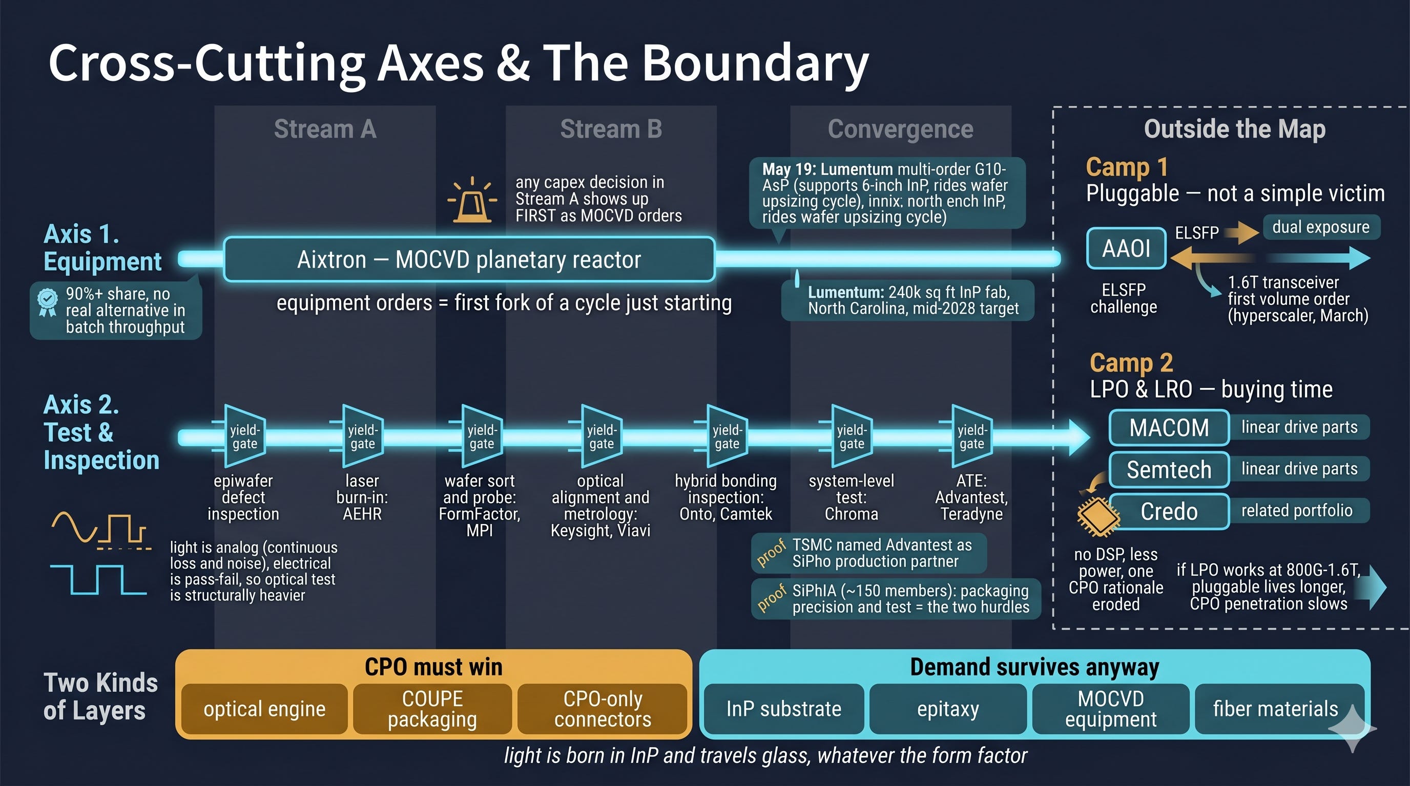
MOCVD for InP epitaxy is a market Aixtron effectively monopolizes with its planetary reactor. The industry puts its share above 90%, and there is no real alternative on batch throughput. The reason equipment matters is position. Whichever layer in Stream A decides to expand, substrate or epi or laser, that decision shows up first as an MOCVD order.
Lumentum’s multiple G10-AsP orders disclosed on May 19 are exactly that signal, and this platform supports InP up to 6 inches, so it rides the wafer upsizing cycle as well. Layer on Lumentum’s plan to spend hundreds of millions of dollars on a 240,000 square foot InP fab in North Carolina targeting mid-2028 operation, and equipment orders are the first inflection of a cycle that has only just begun.
Axis 2. Test/Verification/Inspection
Every seam in CPO is a yield gate, and every gate carries inspection and test equipment. Defect inspection at the epiwafer stage, laser die burn-in (AEHR’s territory), wafer sort and probing (FormFactor, MPI), optical alignment and optical metrology (Keysight, Viavi), hybrid bonding precision inspection (Onto Innovation, Camtek), system-level test (Chroma), and ATE (Advantest, Teradyne).
Electrical signals resolve to pass or fail, but light exists as continuous quantities of loss and noise, an analog domain, so a device with optics in it carries structurally higher test intensity than an electrical device of the same class.
Two public signals show this axis’s standing: TSMC, in naming collaboration partners for SiPho volume production, directly cited test equipment maker Advantest alongside materials and laser companies, and the silicon photonics alliance in Taiwan (SiPhIA), reportedly gathering around 150 members including TSMC and Coherent, defined packaging precision and test as the two main hurdles to volume production.
The Boundary: Pluggables, LPO, and Dual Exposure
Reading attach rate requires looking outside the map too. On the other side stand two camps. One is the pluggable camp. But reading this camp as a simple victim of CPO gets it wrong. AAOI is the prime example: in March it disclosed its first volume order for 1.6T transceivers from a major hyperscaler, while at the same time, as covered above, challenging for the ELS socket with its ELSFP. That is dual exposure, riding the transceiver boom while planting a foot in the light source socket of the CPO era.
The other is the LPO and LRO camp. MACOM’s and Semtech’s linear drive components and Credo’s related portfolio hang here, and the approach of removing the DSP to ease pluggables’ power problem erodes one of the rationales for the CPO transition. If LPO works well enough in the 800G and 1.6T range, pluggable life gets extended and CPO penetration slows by that much.
With this boundary in view, the layers inside the map split into two kinds. Engines, COUPE packaging, and CPO-specific connectors are architecture-dependent layers that only earn if the CPO architecture wins.
By contrast, InP substrates, epi, MOCVD equipment, and fiber materials keep their demand whether pluggables hold out, LPO buys time, or CPO penetrates. Whatever form the light travels in, light is made from InP and rides glass fiber.
This distinction will drive the investment judgments in the second half.
That completes the anatomy of the CPO supply chain: how the light is made, how signal gets loaded onto it, where the two meet, and who stands at each layer.
But a map is a map.
You cannot make money from the map alone. The same map only becomes an investment once you can read which layers the money has already entered and which still sit empty.
From here, I layer onto this map the Silicon Valley stories found in no filing and no IR deck, build six investment theses on top of it, and finally convert those theses into names and weights.