

Why Optics Now
Data center bandwidth requirements have hit 800G and 1.6T, and electrical interconnects can’t keep up. Power consumption explodes, signal integrity collapses, PCB layers keep stacking, and costs spiral out of control. The answer is optics. That much is clear.
But when optics moves into actual manufacturing, it means something different. The moment signals shift from copper to light, testing stops being a simple pass/fail check. It becomes the core process that determines yield and reliability. As optics moves closer to the package, measurement gets harder, and that gap has to be filled with on-chip monitors and system-level validation. This article covers how the shift to optics changes testing methods and structure, and who benefits from that change.
Substack is currently in a trial phase, so all premium quality articles are available for free for now. Once paid subscriptions are introduced, pricing will be set at a level comparable to professional tech writers on Substack. Early supporters will have the benefit of locking in their current pledge price for future paid access.
Optical Communication in One Diagram
An optical link is just a “device that moves bits.” The difference between electrical and optical is what carries those bits: wire or light.
Break an optical link into its simplest form and you get six stages:
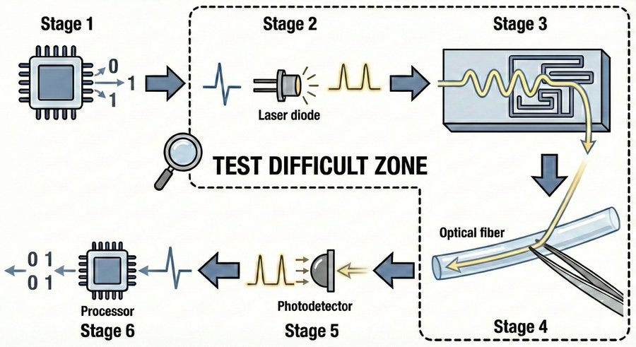
Electrical signal generation: high-speed bits come out of the chip
Driver and modulation: electrical signals shake the laser light to create 0s and 1s
Optical path: light travels through waveguides inside the chip or package
Coupling: light gets “aligned” into fiber or another chip
Reception: photodetector converts light back to electricity
Recovery: analog front-end and DSP reconstruct clean bits
Testing gets hard because stages 2, 3, and 4 move into places engineers can’t easily touch.
Five Reasons Testing Gets Harder with Optics
1) Measurement targets double: electrical and optical
When everything was electrical, you measured voltage, current, jitter, timing. Add optics and you also need OMA, ER, TDECQ, BER, eye diagrams.
Electrical can be fine while optical output fluctuates. Optical can look good while electrical timing drifts. You need two sets of test equipment, correlation analysis, and engineers who understand both domains.
Who makes optical test equipment?
Keysight Technologies (NYSE: KEYS): Offers measurement portfolios that verify both electrical and optical signal quality, including optical modulation quality analyzers like OMA and transceiver test solutions.
VIAVI Solutions (NASDAQ: VIAV): Provides modular optical test gear (power meters, spectrum analyzers, attenuators, switches) optimized for transceiver manufacturing test lines.
2) External testing disappears as optics gets closer
Electrical signals? Probe them or plug in cables.
Traditional pluggables? Connect test equipment to the optical connector.
CPO? Different story. Once the optical path and coupling points move inside the package, external equipment can’t reach them anymore.
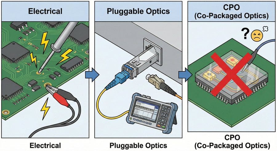
At that point, production floors need three things instead of external measurement:
On-chip loopback
On-chip monitoring and telemetry
End-to-end validation at system level
Testing is no longer just a manufacturing step. It spans design, firmware, and system operations.
Who’s leading CPO?
NVIDIA (NASDAQ: NVDA): Explicitly integrates CPO into ASIC with Spectrum X Ethernet Photonics switches. When optics moves into the package, external measurement can’t manage it alone. Product design has to assume in-package optical links from the start.
Broadcom (NASDAQ: AVGO): Announced Tomahawk 6 Davisson as a CPO Ethernet switch, pushing an architecture built around in-package optics for next-gen AI networking.
3) Alignment and coupling determine yield
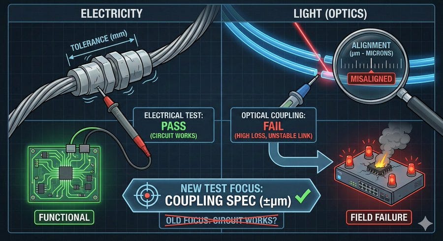
Light is far more sensitive to “alignment” than electricity. Misalignment by a few micrometers increases loss, and increased loss destabilizes the link. Worse, electrical testing doesn’t catch it. A device can pass all electrical tests and still fail in the field if optical coupling is bad.
In the optical era, testing cares less about “does the circuit work” and more about “is coupling within spec.”
Who tackles alignment and assembly challenges?
POET Technologies (NASDAQ: POET): Centers its platform on optical interposer-based integration, assembling optical and electronic devices on a single platform to reduce alignment burden.
Fabrinet (NYSE: FN): Makes precision alignment and assembly processes its core competency in transceiver and optical component manufacturing, controlling the manufacturing stage that determines actual production yield and quality.
4) Temperature and wavelength become fixed test variables
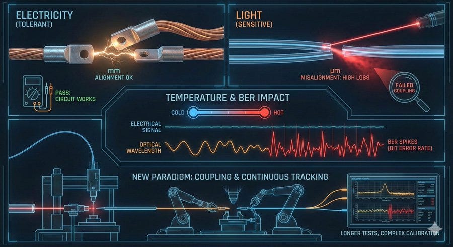
Optical components are temperature-sensitive. Laser output fluctuates, resonant wavelengths shift, and BER (Bit Error Rate) spikes as a result.
Put simply: electrical testing often meant checking “cold, hot, middle.” Optical testing has to include “how does wavelength move with temperature.” Test time gets longer, and calibration verification becomes part of the test.
Who’s strong in lasers and transceiver core components?
Lumentum (NASDAQ: LITE): Provides high-speed modulated light sources like 200G-per-lane EML lasers. Laser and modulator characteristics are inherently sensitive to wavelength, temperature, and drive conditions.
Coherent (NYSE: COHR): Emphasizes core chipsets like silicon photonics modulator driver ICs for 800G and 1.6T pluggables. These chipsets naturally elevate operational variables like wavelength tuning and thermal stabilization into test requirements.
5) Process variation and reliability verification matter more
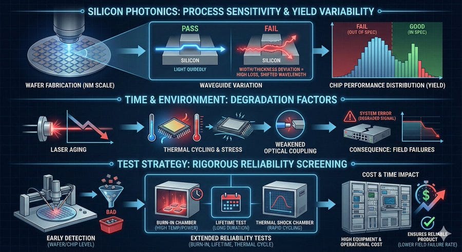
Silicon photonics changes results with tiny process shifts. If waveguide width or thickness varies slightly, light leaks more, loss increases, and wavelength-specific behavior drifts. That’s why chips from the same design show variable optical performance.
Optics also has many elements that change over time. Laser output can gradually decrease or fluctuate. Coupling points can weaken under repeated thermal stress. Package warping or stress alters optical path characteristics.
Production floors need to catch “initially defective products” as early as possible. Burn-in, life testing, and thermal cycling get more emphasis, and the time and equipment costs for these processes heavily influence overall cost structure.
Who handles silicon photonics at the foundry level?
GlobalFoundries (NASDAQ: GFS): Operates a separate silicon photonics platform, managing process variation control and production reliability data in this critical area.
Tower Semiconductor (NASDAQ: TSEM): Expanding its role in the optical process ecosystem through silicon photonics and CPO-related foundry offerings.
Tower Semiconductor: Everything You Need to Know

Silicon photonics foundry. Still an unfamiliar term for many, but right now it’s one of the hottest keywords in the semiconductor industry. A factory that mass-produces chips that transmit data using light. Tower is currently standing at the front of that line. It is the de facto sole volume supplier of 1.6T (1.6 terabits per second) PICs (Photonic Inte…
How Testing Changes at Each Manufacturing Stage
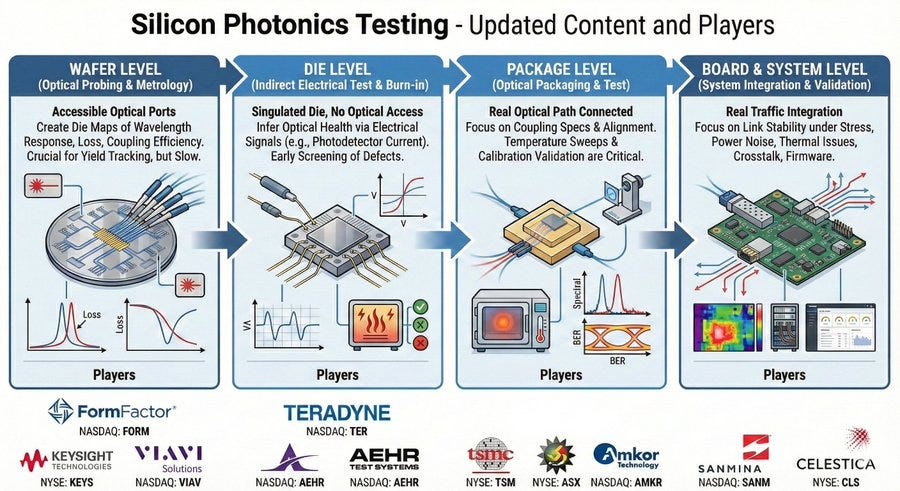
Wafer Stage
Optical ports are relatively accessible at wafer level. That’s why extracting maximum data on wavelength response, loss, and coupling efficiency matters here. This data becomes the per-die “map” and the reference point for tracing yield problems later.
Optical measurement is slow, though. Wavelength sweeps and alignment stabilization are necessary. Prober throughput drops, and “how much to measure” becomes a cost decision.
Key players (optical wafer probing and metrology)
FormFactor (NASDAQ: FORM): Provides optical probes that precisely align to grating couplers and edge couplers on silicon photonics wafers. Core function is automated measurement of resonance wavelength, coupling efficiency, and waveguide loss per die to build “optical characteristic maps.” Without these maps, tracing failure causes at package stage becomes impossible.
Keysight Technologies (NYSE: KEYS): Sweeps wavelengths from 1520nm to 1580nm with tunable lasers to measure ring resonator Q-factor and FSR, tracking wavelength drift across temperature changes. Wafer stage is the last chance to access optical ports, so the optical metrics extracted here become the baseline for yield prediction in downstream processes.
VIAVI Solutions (NASDAQ: VIAV): Provides modular metrology systems for wafer-level optical testing, integrating power measurement, spectrum analysis, and polarization control into production probing environments. Automation and parallel measurement are the differentiators in this throughput-critical stage.
Die Stage
Once you cut wafers and start assembly, direct external access to optical ports gets difficult. At this stage, “directly observing light” isn’t realistic. Inferring optical state from electrical signals is. Photodetector current and similar values quickly screen for anomalies. Even if you can’t see light, you build electrical paths to catch problems fast.
Key players (electrical-based indirect measurement and burn-in)
Teradyne (NASDAQ: TER): Rapidly screens electrical circuits like SerDes, drivers, and TIAs in dies containing optical devices. Core capability is indirect detection of optical device anomalies through electrical signals (photodetector current, laser driver bias) when direct optical measurement isn’t possible.
Aehr Test Systems (NASDAQ: AEHR): Provides high-volume parallel burn-in at wafer and die stages with WaferPak and FOX systems. Optical devices like lasers and photodetectors have high infant mortality rates, so monitoring current-voltage characteristics under temperature stress for early screening is critical to yield. Explicitly includes silicon photonics as a target market.
Package Stage
Package completion creates the first real optical path. From here, “does the circuit work” matters less than “is coupling within spec” for pass/fail decisions. Slight alignment errors increase coupling loss, and links can become unstable even when electrically perfect.
Temperature changes can also shake laser or resonance conditions, so temperature sweeps and calibration verification often consume test time.
Key players (optical packaging and test)
TSMC (NYSE: TSM): Pursuing silicon photonics integration in its 3DFabric platform, working on integrating optical devices into CoWoS-based interposers. Coupling loss and thermal management become yield drivers at the package stage where optical paths are finalized, and advanced packaging experience carries straight into optics.
ASE Technology Holding (NYSE: ASX): Provides both assembly and test for optical transceiver modules, emphasizing turnkey services that include optical coupling alignment, temperature sweep testing, and BER verification. Infrastructure for simultaneous optical and electrical verification at package stage is the differentiation.
Amkor Technology (NASDAQ: AMKR): Lists silicon photonics and optical interconnect packaging explicitly in its advanced packaging portfolio, building capability in CPO and optical module assembly. Yield learning in optical alignment processes separates OSAT competitiveness.
Board and System Stage
Once mounted on boards with real traffic flowing, problems invisible at package stage appear. Power noise, thermal gradients, inter-channel interference, firmware timing all affect link quality. This stage focuses on link stress testing, system-level burn-in, and field telemetry to catch “instability in operating environments.”
Key players (system integration and end-to-end validation)
Sanmina (NASDAQ: SANM): Manufactures optical networking switches and line cards, validating link stability under actual traffic. Catches cases where modules that passed package-stage testing show BER spikes from power noise, thermal gradients, or crosstalk after board mounting. System-level burn-in and environmental stress testing serve as the final gate before shipment.
Celestica (NYSE: CLS): Covers silicon photonics transceiver design through system integration, explicitly mentioning OBO (On-Board Optics) and CPO commercialization. Core engineering validates that firmware calibration, link training, and thermal management work properly when optical modules integrate into actual servers or switches. Validates telemetry functions before field deployment.
Conclusion: The Race Is Yield Learning Speed
The optical transition isn’t just about faster links. Measurement targets expand to include optical metrics alongside electrical ones, and measurement points move deeper inside packages. Testing stops being “final pass/fail at the end” and becomes the core process controlling production cost, schedule, and reliability.
What matters most in the optical era is who finds root causes faster when problems surface, who fixes processes faster, and who updates standards faster.
Many roads lead back to POET...
Thank you for all the content. You make it so easy to understand and have helped me connect the dots. And love your visual diagrams, it’s how I best retain information. 🙂