


On March 2, 2026, NVIDIA invested $2B in Coherent and another $2B in Lumentum. Both companies make lasers. The two announcements came on the same day and included “multi-billion dollar purchase commitments” and “future capacity access rights.” Jensen Huang wasn’t just buying lasers. He was locking up the ability to make them.
Ten days later, on March 12, just before OFC 2026, the world’s largest optical communications conference, three MSAs were announced simultaneously.
AMD, Broadcom, Meta, Microsoft, NVIDIA, and OpenAI showed up in the same room to declare the standard for optical interconnects. Companies that had been fighting each other in the GPU market were suddenly on the same side.
The War of Light Has Begun

On March 12, 2026, three separate optical-related MSAs dropped on the same day. That does not happen by coincidence. It means the entire industry has converged on the same conclusion: the physical layer of AI infrastructure needs to change, and it needs to change now. Call it the opening shot of the Optical War.
Why? Because there aren’t enough lasers. And without lasers, it doesn’t matter how many GPUs you make. You can’t connect them.
If HBM was the bottleneck of 2023 to 2024, lasers are the bottleneck of 2025 to 2027.
And this optical market is more complicated than HBM. There are four types of lasers, various types of modulators, and three form factors. Each combination represents a different technology, a different company, a different investment opportunity.
If you have been investing in optical related stocks without fully understanding what kinds of lasers are actually used, what roles they play, and where the technology is headed, I strongly encourage you to read this article.
From the basic principles of lasers, to the different types of modulators, to the competitive landscape by transmission distance, and the map of the key players, this article covers it all.
After reading it, everything will feel much easier and much clearer to understand.
1. The Limits of Copper, and the Shift to Light
Most of what connects chips inside a data center today is copper cable. But copper has hit a physical wall. Once data transmission speeds reach 200Gb/s per lane, the distance copper can carry a signal without degradation drops to under one meter. “Per lane” refers to a single electrical channel. In practice, transceivers bundle multiple lanes together to build total bandwidth. An 800G transceiver (800 gigabits per second, or 100 gigabytes per second), for example, is built as “200G x 4 lanes” or “100G x 8 lanes.”
The physical housing for these transceivers is called a form factor. The most widely used today is the QSFP-DD (Quad Small Form-factor Pluggable Double Density).
Breaking down the name: SFP (Small Form-factor Pluggable) was originally a single-lane standard. QSFP (Quad SFP) bundles four of them. Add DD (Double Density), and the electrical connector is doubled into two rows, bringing the lane count to eight. Same slot size, twice the bandwidth. It’s hot-swappable, meaning you can plug it into the front panel of a switch and pull it out again. 100G per lane x 8 lanes gives you 800G QSFP-DD. 200G per lane x 8 lanes gives you 1.6T QSFP-DD.
Worth noting: QSFP-DD doesn’t imply optical or copper. It’s just the shell, the form factor. What you put inside is what determines the technology.
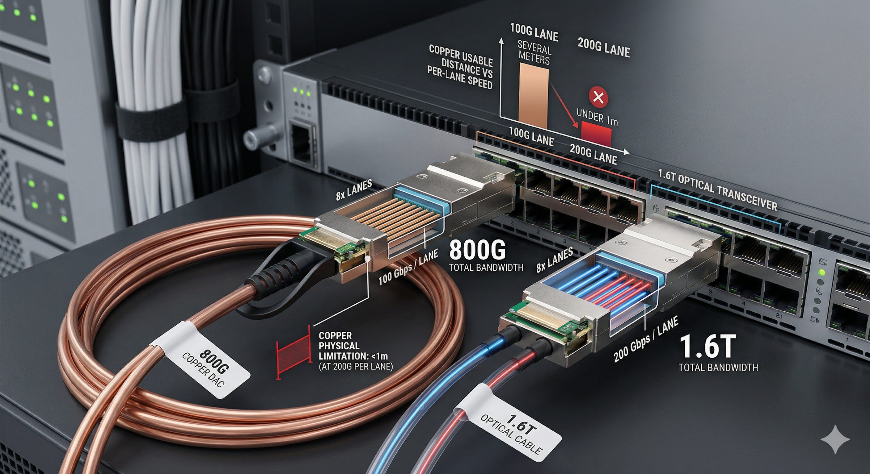
Copper’s problem shows up when you go from 800G to 1.6T and beyond. Once per-lane speed crosses 200G, signal degradation in copper gets severe fast. At 800G, copper DAC cables could cover several meters. At 1.6T (200G x 8 lanes), the usable distance shrinks to under one meter, and even then you need a retimer chip to maintain signal integrity. At 3.2T (400G x 8 lanes), copper struggles with distances measured in centimeters. In the 1.6T world and beyond, optical interconnects aren’t a nice-to-have. They’re the only option.
2. Lasers and Modulators: The Concepts You Need to Know First
What a Laser Does
Inside a data center, a laser does exactly one thing: it generates light. That light travels through optical fiber, bouncing off the fiber walls, covering hundreds of meters or several kilometers. Once you encode data (ones and zeros) onto that light, you can transmit information faster, farther, and at lower power than copper wire.
Here are the three concepts you need to understand:
What a laser is
What optical fiber is
What it means to put data on top of light (more on this in the modulation section)
LASER stands for Light Amplification by Stimulated Emission of Radiation.
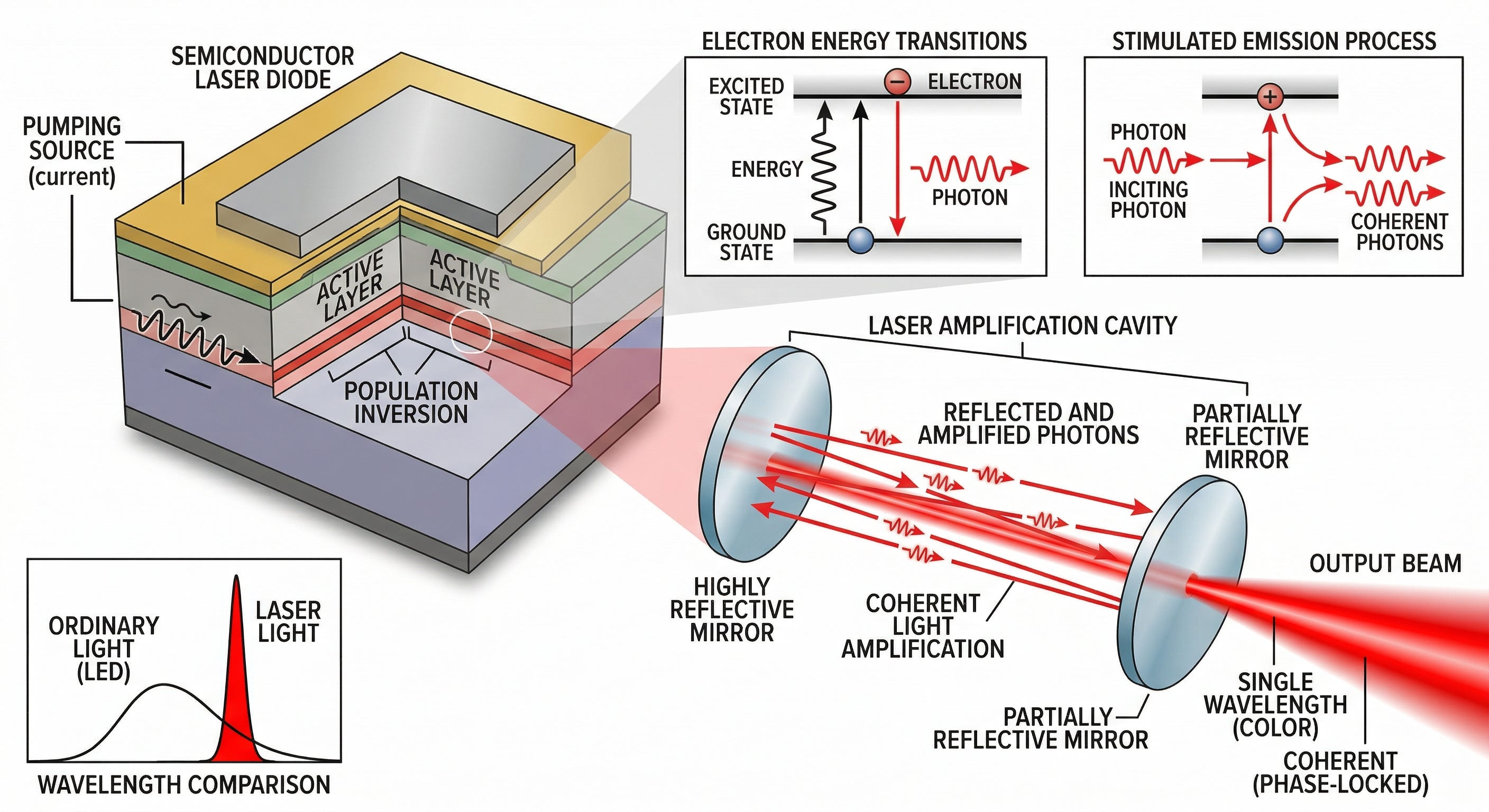
Here’s how it works: when you run current through a certain semiconductor material, electrons absorb energy and jump to a higher state. When they fall back down, they release photons, which is light. Those photons bounce back and forth between mirror-like surfaces inside the chip, amplifying as they go, until they exit through one end. That’s your laser beam. The key difference from an ordinary LED is that a laser emits light at a single wavelength, a single “color.” That precise, coherent light is what makes long-distance transmission possible.
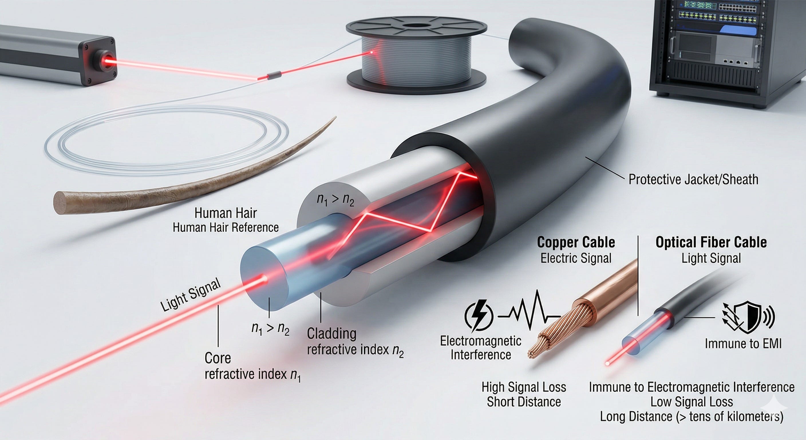
The light a laser generates travels through optical fiber, which is a glass (silica, SiO2) cable drawn thinner than a human hair. At its center is a core where light travels. Surrounding the core is a cladding with a different refractive index. Because the core has a higher refractive index than the cladding, light undergoes total internal reflection inside the core, staying in and propagating forward. Copper carries electrical signals; optical fiber carries light signals. Unlike copper, fiber is immune to electromagnetic interference, and its signal loss is so low that it can carry data for tens of kilometers.
Two Semiconductors, Two Fiber Types
Optical fiber comes in two types depending on core diameter, and which type you use depends on which laser you're running. Data center lasers use two families of semiconductor materials.
And it is commonly referred to as a III-V compound semiconductor.
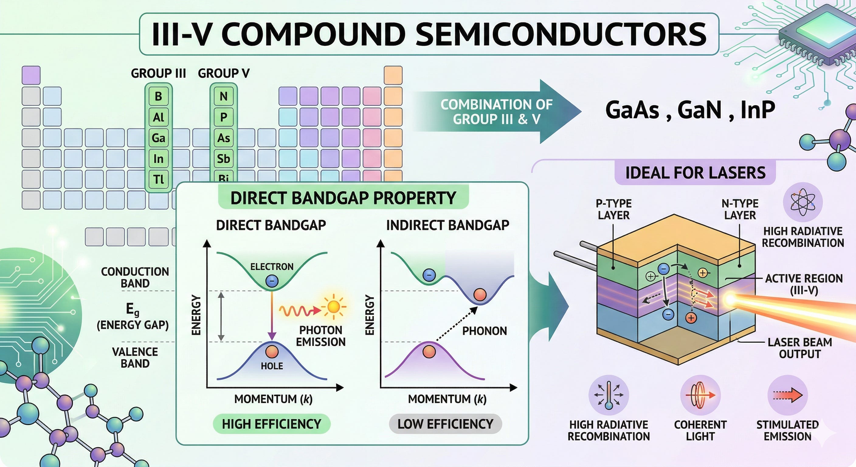
A III-V semiconductor is a compound semiconductor made by combining Group III and Group V elements from the periodic table. These materials have a direct bandgap, which makes them highly efficient at converting electricity into light, so they are very well suited for making lasers.
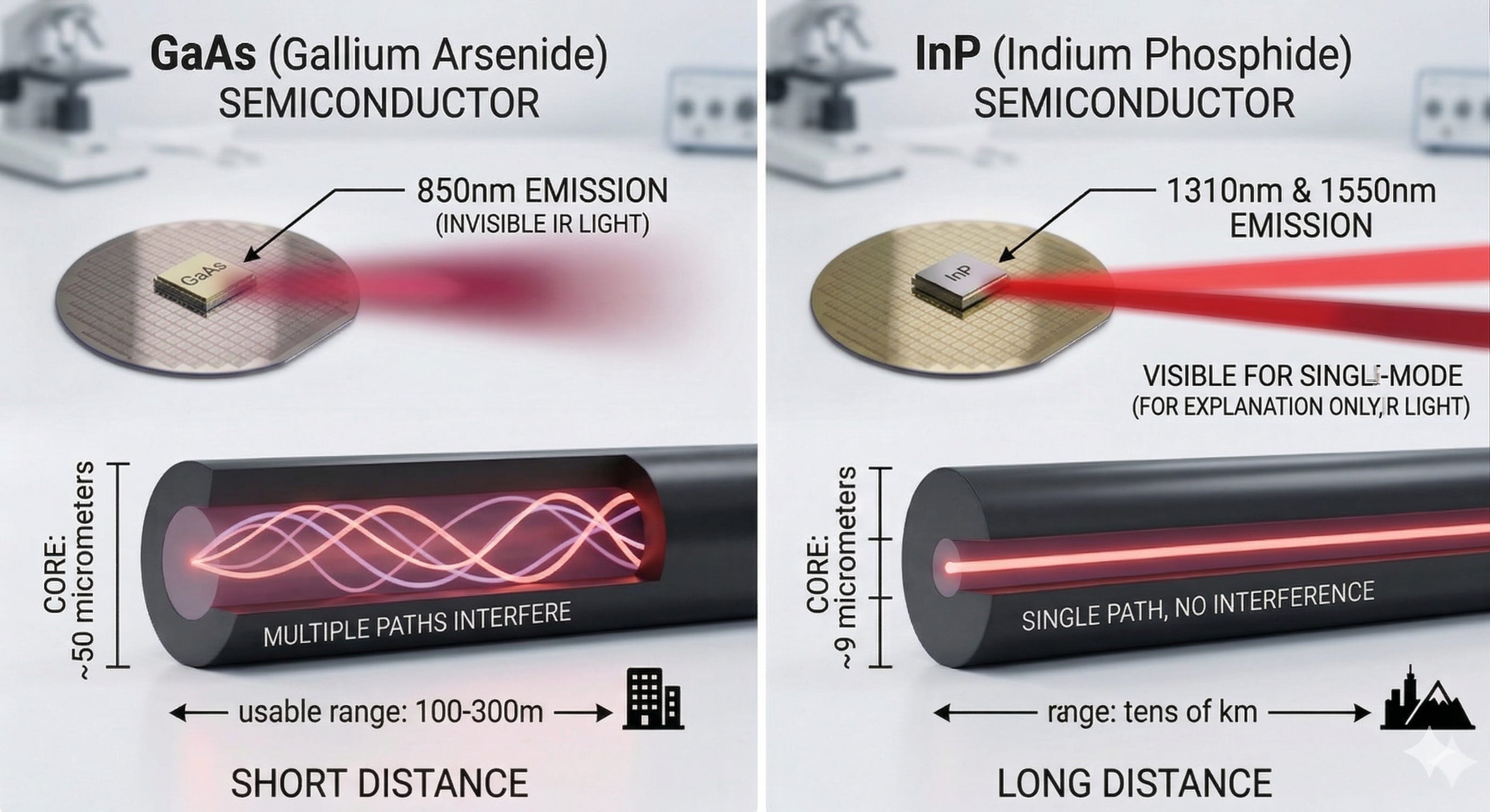
GaAs (Gallium Arsenide): A compound semiconductor made from gallium and arsenic. It emits light at 850nm, in the infrared, invisible to the eye. This wavelength works well in multimode fiber (MMF), which has a relatively wide core diameter of around 50 micrometers, roughly half the thickness of a human hair. A wider core lets light enter at multiple angles simultaneously (hence “multimode”), making it easy to manufacture and align, but the multiple light paths interfere with each other over distance, causing signal degradation quickly. The usable range tops out at 100 to 300 meters.
InP (Indium Phosphide): A compound semiconductor made from indium and phosphorus. It emits at 1310nm or 1550nm, wavelengths optimized for single-mode fiber (SMF), which has a core diameter of about 9 micrometers. With only one path for light to travel, there’s no interference, and the signal can travel several to tens of kilometers without breaking down.
To summarize:
GaAs produces 850nm light, works in multimode fiber, and is used for short distances.
InP produces 1310nm or 1550nm light, works in single-mode fiber, and handles long distances.
Laser Structures: VCSEL vs. DFB
There are two types of lasers used in data centers. They differ in the direction light comes out of the chip, the semiconductor material they’re made from, and the distance they can cover.
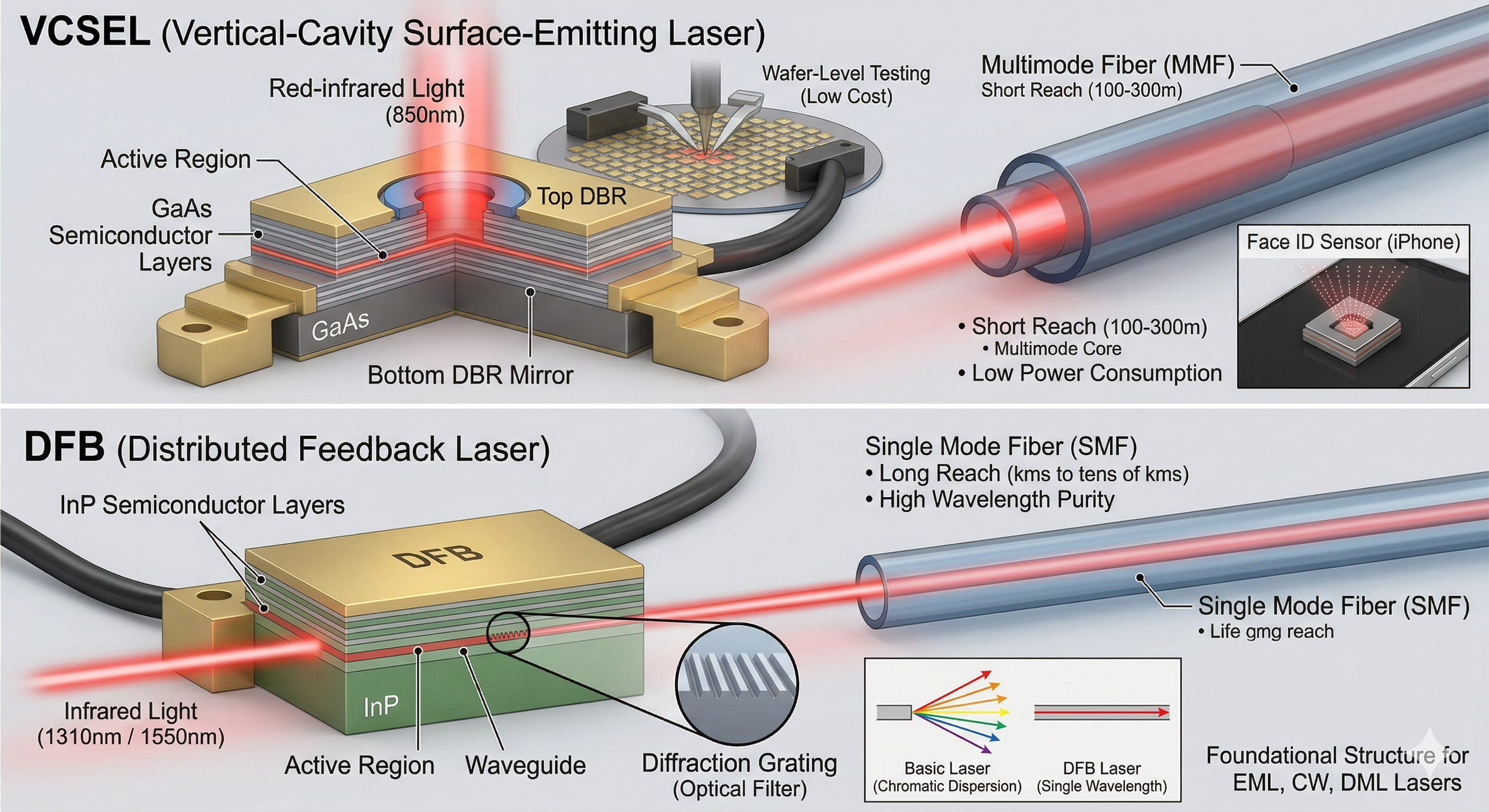
VCSEL (Vertical-Cavity Surface-Emitting Laser)
Light exits from the top of the chip. Made from GaAs, operates at 850nm wavelength, and works exclusively with multimode fiber. Reach is about 100 to 300 meters.
VCSELs have three key advantages.
First, they’re cheap. Because light comes out the top, you can test thousands of chips simultaneously while they’re still on the wafer (the semiconductor disc) before cutting them apart. Catching defects early keeps mass production costs low.
Second, they consume very little power. The distance light travels back and forth inside the chip is extremely short, so it takes very little current to achieve lasing.
Third, the beam comes out in a circular shape, which makes it easy to couple into a fiber.
The most familiar application isn’t in data centers.
It’s the iPhone’s Face ID.
The sensor that projects 30,000 infrared dots onto your face to map it in 3D uses a VCSEL as its light source. Supplying hundreds of millions of VCSELs per year to Apple is how Coherent built its economies of scale, and that manufacturing expertise carried directly into developing high speed VCSELs for data centers.
DFB (Distributed Feedback Laser)
Light exits from the side of the chip, traveling horizontally. Made from InP (indium phosphide), operates at 1310nm or 1550nm wavelength, and works exclusively with single mode fiber. Reach extends from several kilometers to tens of kilometers.
The reason DFB exists comes down to one thing: wavelength purity. A basic laser (called an FP laser, or Fabry-Perot laser) emits multiple wavelengths of light at the same time. When different wavelengths travel together through a fiber, each one moves at a slightly different speed, causing the signal to spread out over distance. This is called chromatic dispersion. Over long distances the signal smears beyond recognition. DFB solves this by etching a fine corrugated pattern called a “diffraction grating” directly into the chip. Think of it as an optical filter built into the laser itself. It selects exactly one wavelength and suppresses everything else. A single wavelength beam is resistant to chromatic dispersion, which is what makes high speed, long distance transmission possible.
The EML, CW laser, and DML that come up later in this article are all built on top of the DFB structure. The only thing that changes between them is how data gets encoded onto the light.
EML: Integrates a modulator right next to the DFB for high-speed, long-distance links.
CW Laser: Runs the DFB at constant output with no modulation at the source, leaving that job to a separate silicon chip.
DML: Drives the DFB by switching the current directly, the simplest approach of the three.
Now, DFB is the foundation of every long reach laser in an AI data center.
Modulation: Various Ways to Put Data on Top of Light
The laser generates light. Now you need to encode digital data, ones and zeros, onto that light. This is called modulation. Turn the light on and you have a 1. Turn it off and you have a 0. That’s the simplest form of modulation, called NRZ (Non-Return-to-Zero): consecutive ones don’t cause the signal to drop back to zero between them, it stays on. One bit per symbol. More complex modulation divides light intensity into four levels, transmitting two bits at once. This is PAM4 (Pulse Amplitude Modulation, 4-level), where 00, 01, 10, and 11 are each represented by a different brightness level.
The key question is where and how modulation happens. That single choice determines a laser’s performance, cost, and use case. There are five modulation approaches that matter in AI data centers.
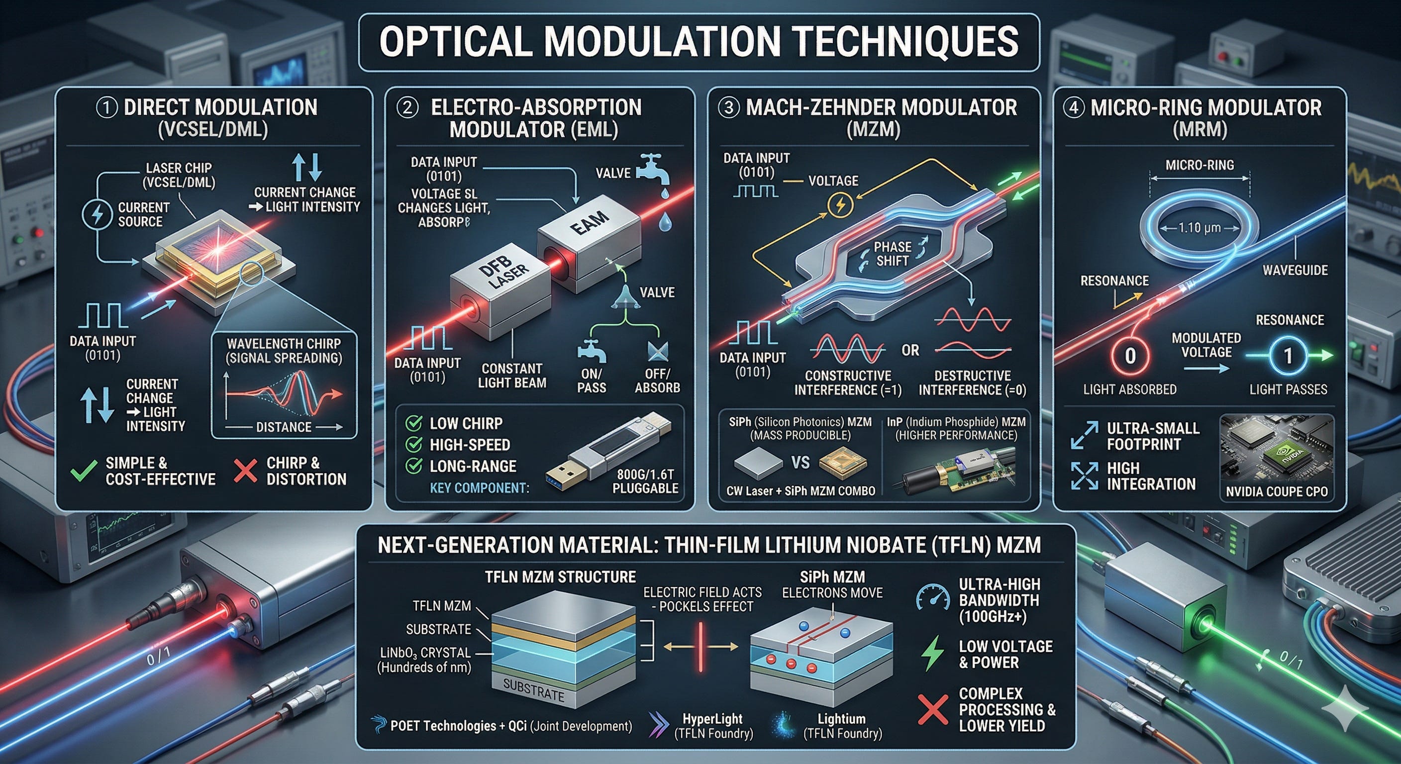
① Direct Modulation: The simplest approach. You rapidly ramp the current flowing through the laser up and down, and the light output follows, getting brighter and dimmer accordingly. No separate modulator chip is needed, which keeps the design simple and cheap. The downside is that when the current changes, the laser’s emission wavelength wobbles along with it. This is called chirp. When chirp is large, the chromatic dispersion problem described earlier gets worse and the signal spreads out over long distances. Both VCSELs and DMLs (Directly Modulated Lasers, which are just DFB lasers operated with direct modulation) use this method.
② EAM (Electro-Absorption Modulator): A modulator built right next to a DFB laser on the same InP chip. The DFB fires a constant beam of light, and the EAM sitting beside it either lets that light pass through or absorbs it depending on the voltage applied, creating the 1s and 0s. Think of the DFB as a faucet that’s always running and the EAM as a valve on the pipe. Open the valve and water (light) flows out. Close it and the flow stops. Because the current driving the DFB stays constant, chirp is minimal, which makes this combination strong for high speed, long distance links.
DFB + EAM = EML (Electro-Absorption Modulated Laser)
It’s the workhorse behind today’s 800G and 1.6T pluggable modules, and it’s also the source of the supply bottleneck.
③ MZM (Mach-Zehnder Modulator): This one splits incoming light into two paths and then recombines them. Apply voltage to one path and the light traveling through it speeds up or slows down slightly (its phase shifts). When the two paths merge back together, if they’re in phase the light comes through strong (= 1). If they’re out of phase the light cancels itself out (= 0). What really matters is what material you build this modulator on. Build it on silicon (SiPh) and you can mass produce it in a standard CMOS fab. Build it on InP and you get better performance.
The combination of a CW laser plus a silicon MZM is rapidly emerging as the main challenger to EML.
④ MRM (Micro-Ring Modulator): A tiny circular ring, just tens of micrometers across, sits next to a straight optical waveguide (the path light travels through). Under certain conditions light gets pulled into the ring and disappears from the main path (= 0). Apply a voltage that slightly shifts those conditions and the light ignores the ring and passes straight through (= 1).
It does the same job as an MZM but in a much smaller footprint, so you can pack more of them onto a single chip.
Built on silicon. This is the modulator NVIDIA plans to use in its TSMC COUPE based CPO.
Both MZM and MRM are primarily built on silicon (SiPh). But a next generation material is gaining serious attention:
TFLN (Thin-Film Lithium Niobate)
The idea is to take a special crystal called lithium niobate (LiNbO₃), slice it into a film just a few hundred nanometers thick, and fabricate an MZM-style modulator on top of it. The modulation method itself is the same as a standard MZM. What changes is the material underneath. A silicon MZM works by physically moving electrons around to alter the speed of light passing through it. TFLN works differently. An electric field acts directly on the crystal structure to change the speed of light (this is called the Pockels effect). No electrons need to move, so the response is dramatically faster. Bandwidth exceeds 100 GHz (silicon MZMs top out at a few tens of GHz), drive voltage is lower, and static power consumption is nearly zero.
It's drawing attention as the modulator material for the 3.2T era, where 400G per lane speeds will be needed.
POET Technologies and QCi are co-developing a 3.2T optical engine based on TFLN, and foundries like HyperLight (US) and Lightium (Switzerland) are already producing TFLN devices. The catch is that this material is difficult to process and manufacturing yields haven't caught up to silicon yet.
Putting Multiple Colors on One Fiber: WDM
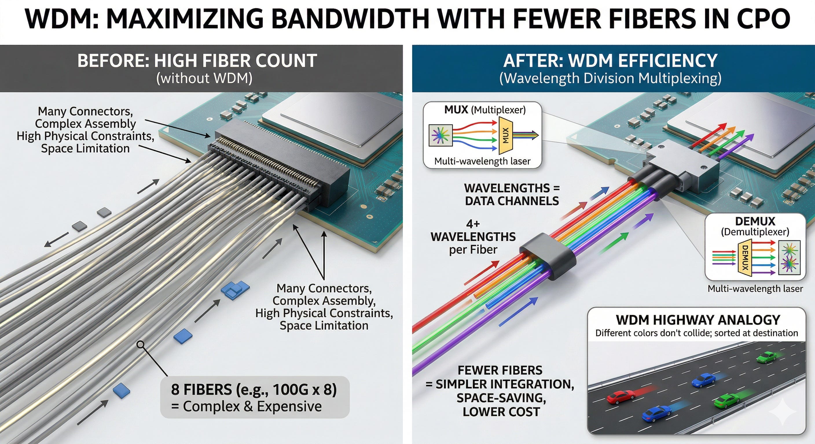
Everything described so far assumes one laser, one wavelength, one fiber. To increase bandwidth, you add more fibers. Sending 800G requires eight fibers (100G x 8). Sending 1.6T also requires eight fibers (200G x 8). More fibers mean more connectors, more space, more cost.
WDM (Wavelength Division Multiplexing) is the solution. Instead of one wavelength per fiber, you put multiple wavelengths on the same fiber simultaneously. Different wavelengths of light don’t interfere with each other inside the fiber, so each one carries its own independent data stream. On the receiving end, filters separate the wavelengths and recover each signal individually. Think of it like a highway where red cars, blue cars, and green cars all travel at the same time. Different colors don’t collide, and at the destination you sort them by color.
With WDM, the same number of fibers can carry several times the bandwidth. Put four wavelengths on one fiber and two fibers do the work of eight. Fewer fibers means fewer connectors, simpler assembly, and less space consumed. In CPO, attaching dozens of fibers directly to a chip is physically difficult, and WDM directly alleviates that constraint.
WDM requires lasers that emit multiple wavelengths simultaneously. That’s the reason multi-wavelength lasers from companies like Scintil, Ayar Labs, Ranovus, and Xscape matter so much in the CPO roadmap.
3. The Battlefield Map: Who Uses What, Where, and How
The laser structures and modulation approaches covered above play out in actual data centers through specific combinations. To understand them, you need to look at three axes simultaneously:
Where it’s used (application)
What form it takes (form factor)
What laser and modulator combination it uses (technology).
At every intersection of these three axes sits a different technology, a different company, a different investment opportunity.