

Silicon photonics foundry. Still an unfamiliar term for many, but right now it’s one of the hottest keywords in the semiconductor industry. A factory that mass-produces chips that transmit data using light. Tower is currently standing at the front of that line. It is the de facto sole volume supplier of 1.6T (1.6 terabits per second) PICs (Photonic Integrated Circuits), and it serves as the primary foundry for both pluggable transceivers and CPO (Co-Packaged Optics, the next-generation technology that places optical modules inside the chip package).
This article covers what Tower does, why the stock is surging, where it sits in the optical foundry competitive landscape, and how I see this company as an engineer who has worked inside foundries. Along the way, I’ll also bring in what I’ve heard directly from people working inside the industry.
Disclaimer
This article is not investment advice. All investment decisions are the sole responsibility of the reader.
1. What Does Tower Semiconductor Actually Do
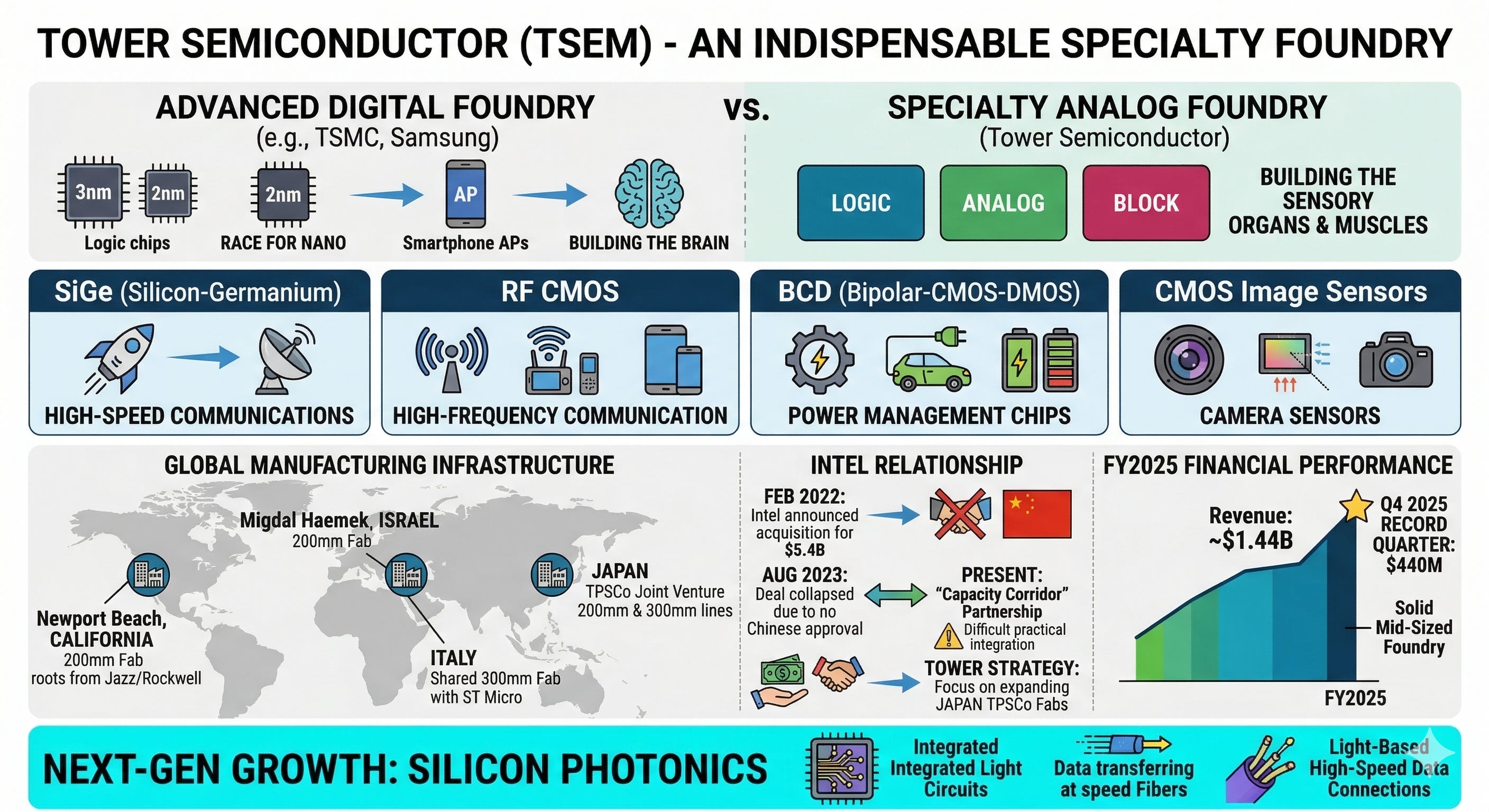
Tower Semiconductor (TSEM) is an Israeli-headquartered semiconductor foundry. A foundry doesn’t design chips itself; it manufactures chips designed by other companies. Samsung and TSMC are the most recognizable examples, and those two companies primarily produce ultra-fine digital chips: smartphone APs, AI accelerators, the kind of products locked in a race to 3nm, 2nm.
Tower doesn’t play that game. What this company does well is what the industry calls “specialty analog”: SiGe (silicon-germanium, a material for high-speed communications), RF CMOS (high-frequency communication chips), BCD (power management chips), and CMOS image sensors (camera sensors). Think of it this way: if the digital world’s giants build the “brain,” Tower builds the “sensory organs” and “muscles” that handle electrical signals, detect light, and regulate power.
Its fabs are distributed across the globe. There’s a 200mm fab in Migdal Haemek, Israel; a 200mm fab in Newport Beach, California (the former Jazz Semiconductor facility, which has roots going back to Rockwell); and fabs in Japan through a joint venture called TPSCo running both 200mm and 300mm lines. In Italy, Tower shares a 300mm fab with ST Microelectronics.
The Intel relationship deserves a direct mention. In February 2022, Intel announced it would acquire Tower for $5.4B. The deal collapsed in August 2023 after failing to clear Chinese regulatory approval. The fact that Intel was willing to spend $5.4B to acquire Tower is itself proof of how irreplaceable its specialty analog technology and fab infrastructure are. After the merger fell apart, the two companies maintained a partnership called a “capacity corridor,” but according to industry sources, the practical integration of their different process systems has been difficult to execute. Intel has acknowledged challenges in fulfilling the arrangement. Tower, rather than depending on Intel, appears to have redirected its strategy toward expanding its Japanese TPSCo fabs.
FY2025 revenue came in at approximately $1.44B. Q4 2025 revenue hit $440M, a record quarter. By this point alone, Tower looks like a solid mid-sized foundry.
But the reason the market is excited about Tower right now is something else entirely: silicon photonics.
2. Why the Stock Is Surging
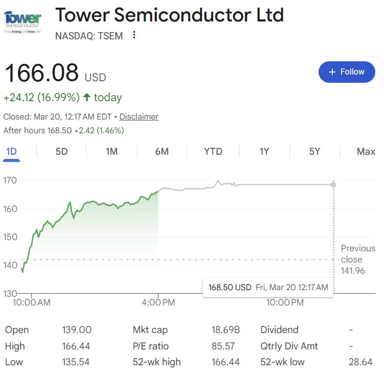
The biggest catalyst dropped on February 5th. Tower announced a collaboration with NVIDIA on 1.6T silicon photonics. Silicon photonics means placing optical components (devices that generate, modulate, and detect light) on silicon so that data can be transmitted using light instead of electricity. The announcement said Tower’s SiPho technology would be used in NVIDIA’s AI datacenter networking, and the stock jumped 12.6% that day.
In March, partnership announcements came every week: Oriole Networks (ultra-low-latency optical switching for AI), NLM Photonics (next-generation optical modulator validation), Lightwave Logic (high-speed polymer modulator PDK integration), Salience Labs (photonic switching for large-scale AI infrastructure), and Xscape Photonics (a startup backed by NVIDIA and Cisco that demonstrated on-chip multi-wavelength lasers). All of it runs on Tower’s PH18 platform.
The timing is sharp. OFC 2026 (Optical Fiber Communication Conference, the largest event in the optical communications industry) is running March 17 through 19 in Los Angeles, and Tower is there presenting its SiPho roadmap. Tower’s message at OFC 2026 is clear: “Our platform covers both Scale-Out (rack-to-rack connectivity) via pluggable transceivers and Scale-Up (intra-server GPU-to-GPU connectivity) architectures via CPO.”
The numbers back the story up. Q4 2025 revenue of $440M was up 14% year-over-year, with net income of $80M beating expectations. More importantly, look at the silicon photonics revenue trajectory: SiPho revenue roughly doubled from approximately $106M in FY2024 to $228M in FY2025. Adding SiGe, the combined SiPho plus SiGe revenue went from $241M in FY2024 to $421M in FY2025. These two technologies now account for roughly 30% of Tower’s total revenue, and that share is climbing fast.
Management is going all-in. What was originally a $650M investment plan for SiPho and SiGe has been raised to $920M, a 40% increase. The target is to grow monthly SiPho production capacity fivefold by Q4 2026 versus the prior year. More than 70% of new SiPho capacity is already reserved by customers through 2028.
The factory isn't fully built yet and the seats are already filled. A contact of mine who works at Tower tells me the volume surge has been dramatic enough that the team is genuinely stretched thin right now. Industry sources corroborate this: fab utilization is near full, with a backlog stretching years out.
3. What TSEM Actually Builds: PIC, EIC, and 3D Stacking
Tower builds three things.
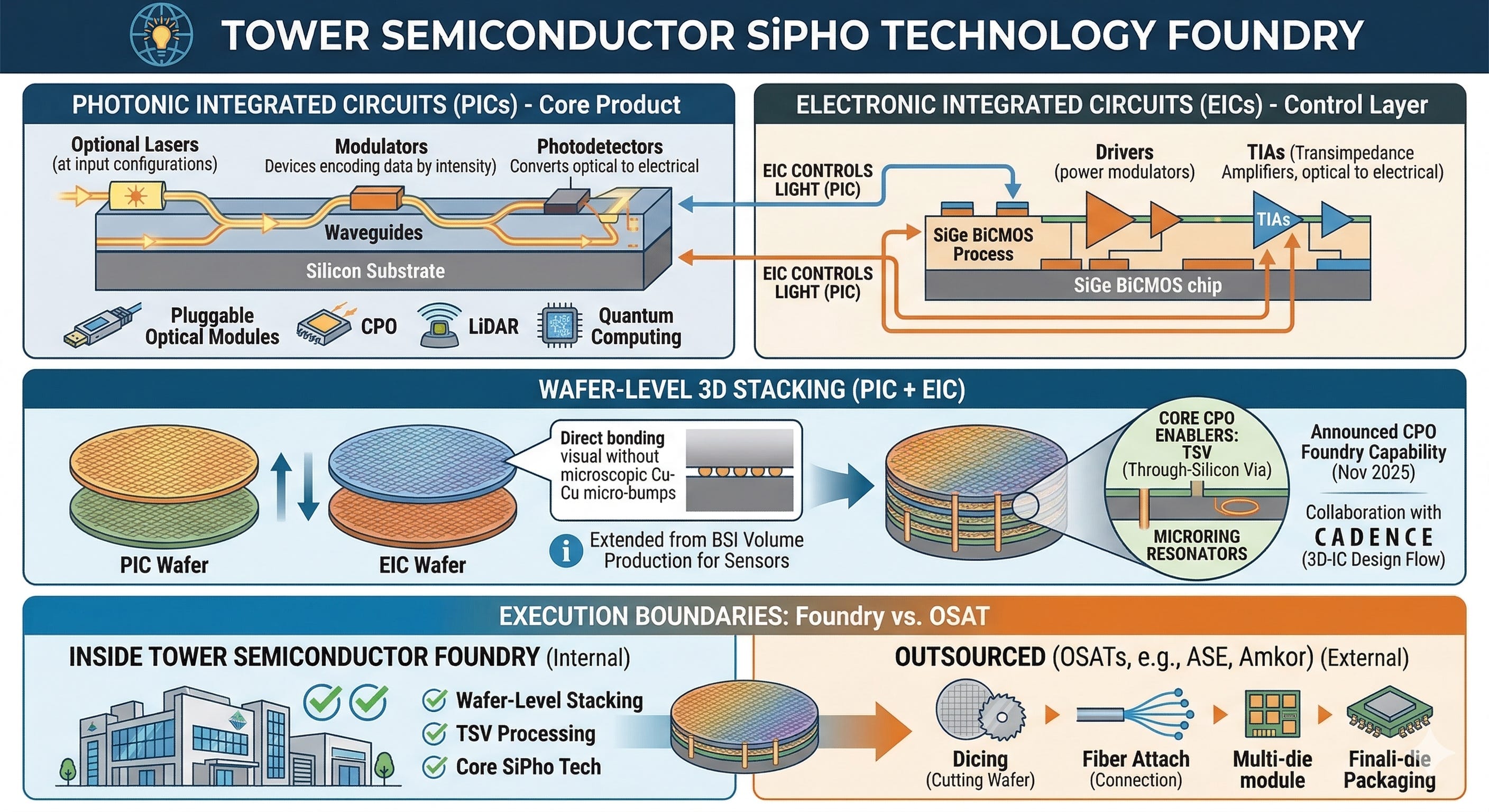
First, PICs (Photonic Integrated Circuits). This is the core product. On silicon, Tower places waveguides (light pathways), modulators (devices that encode data by modifying the intensity or phase of light), photodetectors (devices that convert optical signals back to electrical signals), and in some configurations, lasers. These PICs go into pluggable optical modules, CPO, LiDAR, and quantum computing applications.
Second, EICs (Electronic Integrated Circuits). These are chips made using Tower’s SiGe BiCMOS process: drivers (circuits that power the modulators) and TIAs (transimpedance amplifiers, which convert optical signals to electrical). If the PIC handles the light, the EIC controls it.
Third, wafer-level 3D stacking of PIC plus EIC. Tower took the 3D wafer bonding technology it has run in volume production for camera sensors (BSI, Back-Side Illumination) and extended it to SiPho and SiGe. A PIC wafer and an EIC wafer are bonded vertically into a single 3D-IC. Tower formally announced this CPO foundry capability in November 2025 and built out a 3D-IC design flow together with Cadence. Core CPO enablers like TSV (Through-Silicon Via) and microring resonators are also part of the platform.
What Tower does not do is final module assembly. Wafer-level stacking of PIC and EIC happens inside the fab, but everything after that, including dicing (cutting the wafer into individual chips), fiber attach (connecting optical fiber to the chip), and final packaging, goes to OSATs (outsourced semiconductor assembly and test companies like ASE or Amkor).
What is PH18
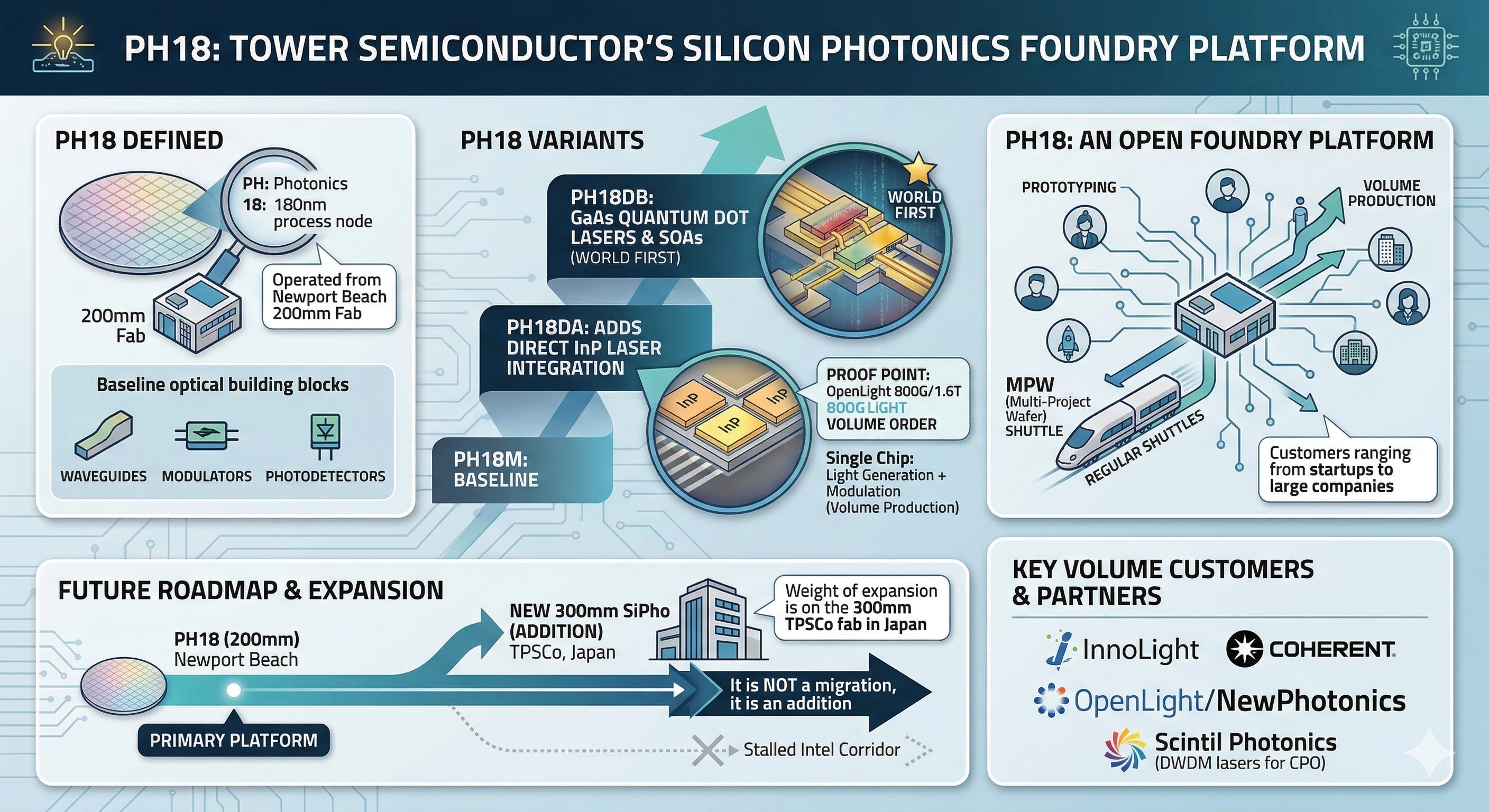
Now for the PH18 platform specifically. PH18 is Tower’s silicon photonics foundry platform, operated out of its Newport Beach 200mm fab. “PH” stands for Photonics, “18” refers to the 180nm process node. Several variants exist.
PH18M (Metal) is the baseline. It provides the core optical building blocks: waveguides, modulators, photodetectors. PH18DA adds direct integration of InP (indium phosphide) lasers on silicon. OpenLight used this PH18DA platform to receive the first volume production order for laser-integrated 800G and 1.6T PICs. It proves that a single chip can both generate light and modulate it for data transmission, without an external laser source, and do it in volume. PH18DB goes further, integrating GaAs quantum dot lasers and SOAs (semiconductor optical amplifiers), a world first.
The defining characteristic of PH18 is that it is an open platform. Any fabless company that designs chips can come to Tower and manufacture on this platform. Tower runs regular MPW (Multi-Project Wafer) shuttles, allowing customers ranging from startups to large companies to prototype quickly and transition directly to volume production.
Current volume customers running on Tower include InnoLight (the world’s largest optical transceiver company), Coherent, and OpenLight/NewPhotonics. Tower is also working with Scintil Photonics on volume production of DWDM (Dense Wavelength Division Multiplexing) lasers for CPO on the Tower platform.
In late 2024, Tower also released a 300mm SiPho process as a standard offering. This is not a migration away from 200mm to 300mm. Tower is keeping PH18 on 200mm as the primary platform and adding 300mm as an option. With the Intel capacity corridor effectively stalled, Tower is placing the weight of its capacity expansion on the 300mm fab expansion at TPSCo in Japan.
4. The Optical Foundry Map: How Tower, TSMC, and GF Differ
Who manufactures silicon photonics chips? Answering that question requires separating out what is being made. An optical system has multiple layers: the PIC die, the EIC die, the integration of those two, and final packaging. Each foundry covers a different portion of that stack.