

1. NVHBM Is Not a New HBM. It Is a Shift in Who Owns the Design
NVIDIA disclosed NVHBM on August 26, 2026. It said it would put a custom memory controller into the HBM base die and let multiple memory providers supply the same NVHBM specification. Versus standard HBM4E it cited up to 30% higher stack bandwidth, up to 15% lower HBM power and up to 25% more XPU compute die area.
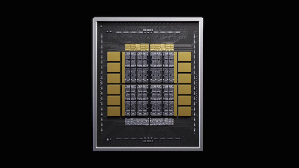
People outside the semiconductor industry sometimes read the name and assume NVHBM is a new form of HBM.
It is not.
The industry calls the HBM we normally refer to standard HBM, or sHBM, and calls the products whose base die is tailored to a customer’s requirements cHBM, or custom HBM. Research and development on cHBM has been under way for years. NVHBM is simply the cHBM NVIDIA uses.
The reason NVHBM deserves attention is not that it is technically special.
It is that NVIDIA defines its own cHBM specification, namely the controller and interface that sit in the base die, and intends to have multiple memory suppliers build to that same structure. In other words, the domain memory vendors used to design together with their customers moves wholesale into NVIDIA’s platform layer. That is where its significance lies. Section 4 onward covers this in detail. First, though, we look at why cHBM emerged and what it means for memory vendors.
2. The Faster HBM Gets, the More the XPU Pays
HBM has raised bandwidth in two ways: widening the interface between XPU and HBM, and running each signal faster. The interface went from 1,024-bit in HBM3E to 2,048-bit in HBM4, and pin speed keeps climbing.
The problem is that HBM does not bear the cost of higher bandwidth alone. A wider interface requires more PHY and I/O circuitry on the XPU as well, and consumes more die edge and more interposer routing. Higher signal rates add power and signal-integrity burden on top.
In an AI accelerator this cost matters more. The XPU’s leading-edge silicon is an expensive resource that should go to compute and cache wherever possible. Yet the more HBM bandwidth rises, the larger the share of that area and power budget the memory interface takes.
So the problem after HBM4 is not solved by making DRAM itself faster.
What is needed is
an architecture that delivers the same bandwidth using less XPU area and power.
That is where the value of an advanced-logic base die and a custom interface comes from.
3. cHBM Reduces That Cost While Creating a New Source of Revenue and Profit
The main disclosed direction for cHBM is to move part of the memory-related logic out of the XPU and into an advanced-logic base die, and to redefine the XPU-to-HBM interface to fit the system. That frees some of the area the HBM PHY and controller occupied on the XPU, and lets the recovered silicon and power budget go back to compute or cache.
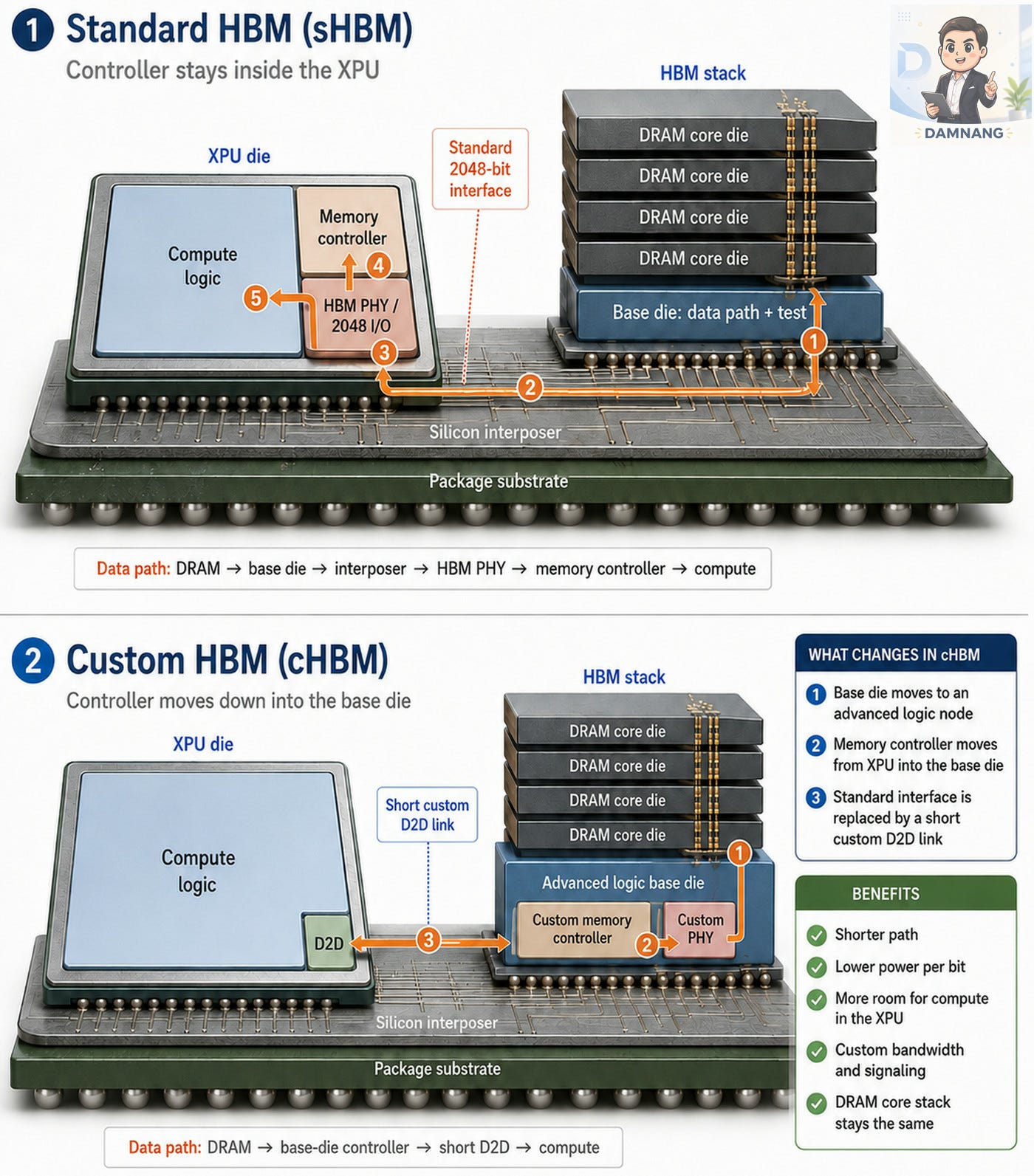
For memory vendors this creates a new value pool. In standard HBM, DRAM die, stacking, test and qualification accounted for most of the product value. In cHBM, base-die design, controller and PHY IP, verification, NRE and customer-specific optimization can be added on top.
Micron’s stated expectation that a customized HBM4E base logic die will carry a higher gross margin than standard HBM4E points the same way. cHBM is not simply faster HBM. It is a product through which memory vendors can sell more engineering value.
4. NVHBM Can Redistribute cHBM’s Value Capture Toward NVIDIA
Throughout this article, custom HBM whose architecture is designed anew for each customer is called bespoke cHBM, and the model in which a platform owner such as NVIDIA sets the spec and multiple suppliers build the same structure is called platform-defined cHBM.
In bespoke cHBM, base-die architecture and qualification can differ by supplier. Once controller, PHY and base die have been designed with one memory vendor, switching to another requires redesign and revalidation. That switching cost is an important reason memory vendors can defend custom design premium and customer relationships.
NVHBM changes this structure. Instead of memory vendors building different cHBM architectures with each customer, NVIDIA defines the controller and interface and multiple memory providers supply the same NVIDIA implementation.
That also changes where the new logic value in an HBM stack accrues. In bespoke cHBM, a memory vendor can go deeper into base-die design, controller, PHY and customer-specific logic and capture proprietary design value. Under NVHBM, NVIDIA defines much of the architecture, so memory vendor differentiation is likely to shift toward DRAM performance, stacking, yield, power and manufacturing execution.
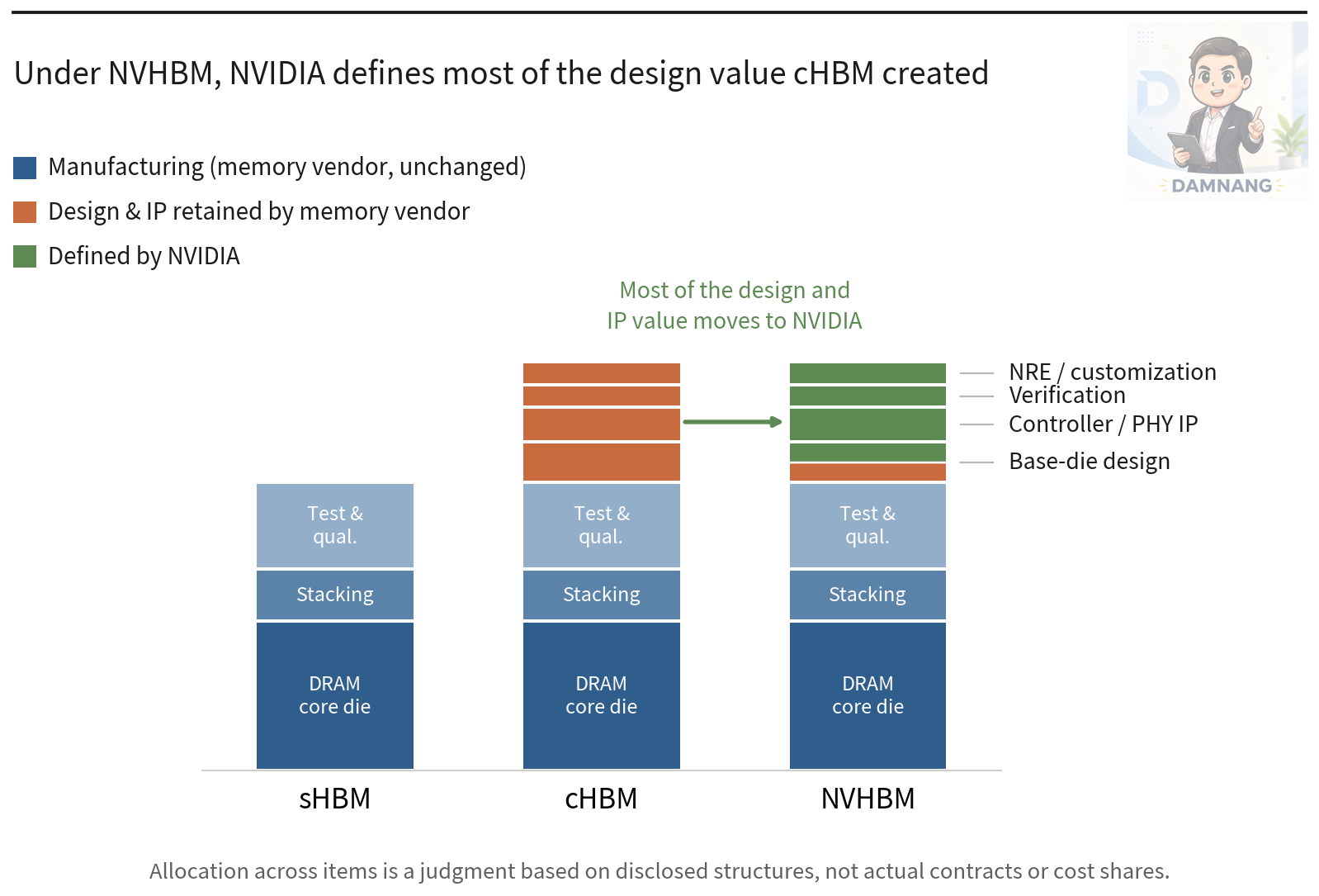
Multi-sourcing reinforces the shift. When several suppliers meet the same NVHBM specification, NVIDIA can qualify suppliers against more common criteria and allocate volume accordingly.
That does not mean memory vendors become fully interchangeable or that prices automatically fall. HBM still differs meaningfully by supplier in capacity, yield, speed, power and thermal behavior, and supply itself remains constrained.
Even so, a common architecture works in the direction of lowering supplier-specific switching barriers. The net effect is that NVHBM increases NVIDIA’s influence over custom memory architecture and supplier selection, and can move part of the design value memory vendors could capture in bespoke cHBM toward the platform owner.
5. What NVIDIA Is Optimizing Is Not HBM but the Whole AI System
Taken separately, density despec and NVHBM look like HBM optimization. The scope NVIDIA is drawing is wider than that: binding compute, memory and interconnect into a single AI factory architecture rather than treating them as separate components.

Density despec lowers memory capacity per accelerator but lets a constrained DRAM supply produce more HBM stacks. All else equal, moving from 12-Hi to 8-Hi raises the number of stacks buildable from the same DRAM die output by a theoretical factor of 1.5. At the same time, demand for base-die units, one per stack, rises.
In NVHBM, NVIDIA directly defines the architecture between XPU and HBM. Outside that, NVLink and NVSwitch handle Scale-Up while Spectrum-X and InfiniBand handle Scale-Out. NVIDIA has added Scale-Across, Context Memory and BlueField-4-based Scale-In to frame the AI factory as five infrastructure pillars. As rack and data center scale grow, optical connectivity grows in importance alongside them.
Add NVLink Fusion and NVIDIA does not need to build every piece of compute silicon itself. Custom XPUs and CPUs are allowed, while memory, the scale-up fabric and the MGX rack architecture still connect into the NVIDIA platform. Amazon Annapurna Labs being named the first NVHBM collaborator, with NVLink Fusion support signaled from Trainium4, shows this strategy is aimed at custom XPUs beyond NVIDIA’s own GPUs.
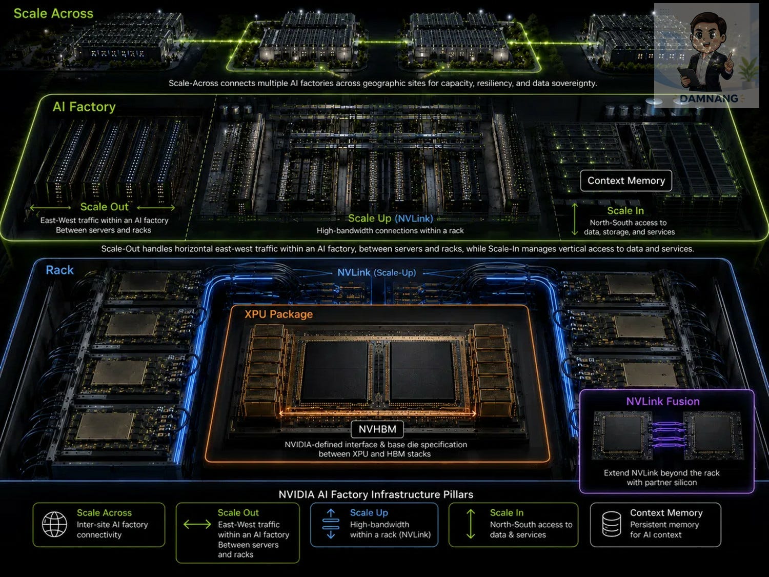
What NVIDIA is expanding is not just GPU share but the scope of the AI system whose architecture it defines. From the GPU out to HBM, rack-scale interconnect, networking, context memory and infrastructure access, that boundary keeps widening. NVHBM is one step in bringing the memory layer inside the NVIDIA platform.


That is how the market reads NVHBM today: NVIDIA takes the spec and keeps widening the scope it defines. Most commentary stops here.
So are memory vendors simply losing ground? No.
This is not the last round. Memory vendors are already preparing for the next one, and in that round there is one position left where what NVIDIA has taken can be won back. It is a domain that cannot be pinned down in a specification, which is exactly why it resists commoditization. Look at where Samsung and SK hynix are putting people and money right now and the direction becomes visible.
The same shift also does not land on all three memory vendors the same way. Set a few conditions, run the numbers per accelerator, and a variable emerges that moves profit far more than design ownership itself. How sensitive that variable is, and how far down the value chain the change carries, is what the rest of this analysis quantifies.
The era of reading HBM through bit growth is ending. What to watch and what to verify in the next cycle starts here.