

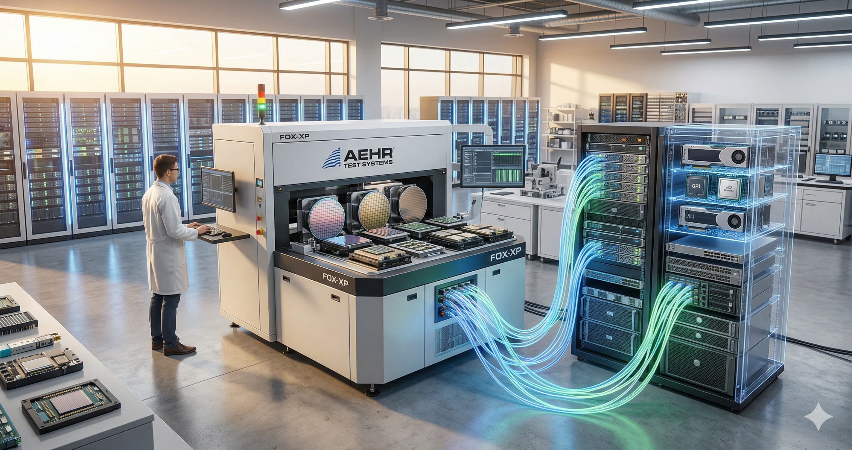
The economics of early-stage semiconductor failures are changing fast. As AI data centers scale and optical interconnect architectures move from roadmap to reality, burn-in, once a process reserved mainly for high-reliability applications, is back at the center of manufacturing strategy. AI processors, silicon photonics, and advanced packaging are all converging to drive this shift.
AEHR is right at the middle of it.
This article draws on my own experience in test, yield, and post-silicon debug work across both foundry and fabless environments. The goal is to explain why burn-in test is regaining strategic importance in the age of AI processors and silicon photonics, and why AEHR is emerging as one of the clearest structural beneficiaries of that shift.
Table of Contents
What Burn-In Is, and Why It Matters Again Now
How Silicon Photonics, Hybrid Bonding, and 3D Stacking Amplify Burn-In Demand
AEHR’s Products and Technical Moat
Business Structure and Profitability
Market Opportunity
Risks
1. What Burn-In Is, and Why It Matters Again Now
The semiconductor test flow after wafer sort, simplified, looks like this.
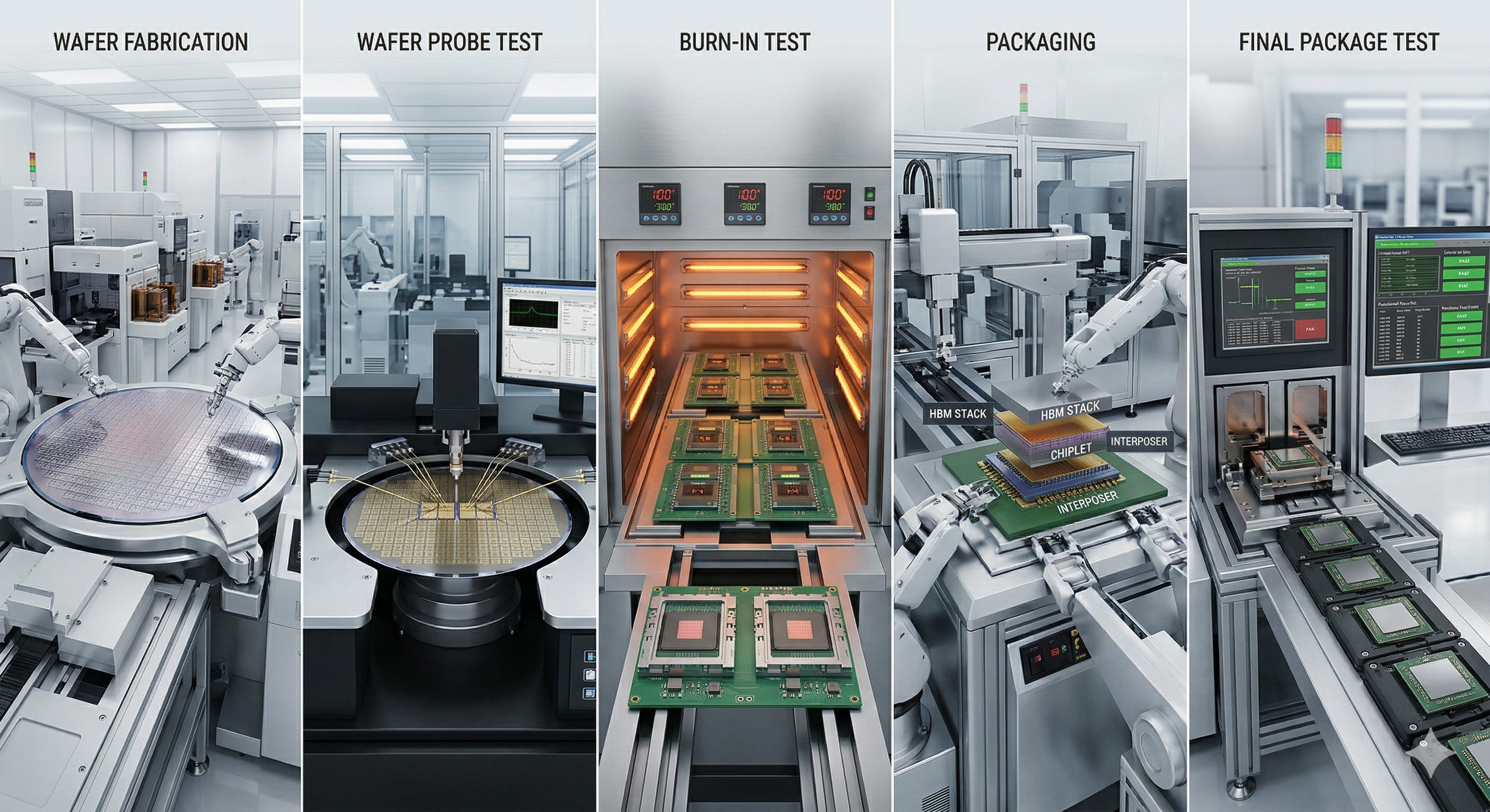
Step 1: Wafer fabrication
The foundry prints hundreds or thousands of identical die across a silicon wafer. Everything stays on the wafer until the individual chips are singulated later in the process.
Step 2: Wafer probe test
Probes make contact with the pads on each die while it is still on the wafer, checking for basic functional operation. Completely dead die and obvious electrical failures get caught here. Probe test is optimized for speed and electrical verification, though, which means it is not designed to catch defects that look fine today but will fail under real-world operating stress over time.
Step 3: Burn-in test
Elevated temperature and voltage stress are applied to the chip for a defined period, intentionally accelerating failures that would otherwise only show up later in the field. Think of it as weeding out parts that pass today but would not survive actual operation.
Step 4: Packaging
Die that pass screening go into the package. This stage has become significantly more complex as CoWoS, HBM stacking, and chiplet integration have grown as a share of the mix.
Step 5: Final (package) test
The packaged part gets tested again to confirm it is ready to ship. This step checks for any issues introduced during assembly and validates end-product functionality.
How Do We Actually Test Semiconductors?

Have you ever wondered how semiconductor testing actually works?
When I was doing yield improvement work, there was a problem I ran into constantly while digging through wafer sort data. Die that passed probe would fail at final test after packaging. Or they would pass final test and come back as customer returns (called as RMA). Failure analysis usually pointed to the same root cause: latent defects.
What is Latent defect?
A hidden defect that does not surface during initial test but converts to an actual failure over time when the device is exposed to heat and voltage stress in real operating conditions.
Classic examples include weak gate oxide, voids inside vias, or metal lines vulnerable to electromigration. Under short room-temperature testing, these all look fine. But under accumulated thermal and electrical stress, they fail, sometimes within hours, sometimes after hundreds of hours.
Burn-in test can catch a significant portion of these defects before they reach the field. It has always mattered, but historically the emphasis was concentrated in automotive and other high-reliability segments. Applying burn-in to every chip is expensive and time-consuming, and for the AP products I was working with, the more common approach was to run burn-in reactively: reproduce a field failure in the lab, trace it back to a process issue, and drive an improvement.
The situation is different now.
Blackwell-class AI GPUs are already operating above 1 kW, and the trajectory points higher. The problem is not just higher power consumption. Higher power means higher current density and more thermal stress inside the die. The faster a latent defect converts to a real failure under operating conditions, the more valuable early screening becomes. That dynamic makes burn-in qualitatively more important for AI accelerators than it was for previous product generations.
Silicon photonics adds another dimension. Here, the case for burn-in is not just about electrical latent defects. Photonic devices that include a transmitter go through an output drift period early in operation, where optical power and wavelength are not stable. Aging the device under controlled current and temperature stress accomplishes two things at once: die with latent defects fail out, and the surviving die have their optical characteristics stabilized through the drift period. For conventional logic, burn-in is purely a screening process.
For silicon photonics, it is simultaneously a screening process and a pre-production stabilization step.
That dual function makes burn-in qualitatively more embedded in the silicon photonics manufacturing flow.
Advanced packaging raises the stakes further. When a defective die ends up inside a CoWoS package or a hybrid-bonded 3D stack, the failure is no longer a single die loss. It can take down the entire package or the entire stack. As integration moves toward CPO architectures that combine optical die and switch ASICs in a single package, a defect in one photonic die can become a system-level loss. Sorting known-good die before packaging is no longer just a cost-saving measure. It is the mechanism that protects yield and unit economics across the full assembly chain.
This is where WLBI, wafer level burn-in, comes in. It is the capability that lets manufacturers screen for known-good die at the wafer stage, before packaging locks in the cost. And beyond the wafer stage, there is PPBI, packaged part burn-in, which applies burn-in stress to the completed device after packaging.
AEHR currently offers solutions in both WLBI and PPBI, and holds a leading position in both AI processor and silicon photonics markets.
What makes the business model structurally interesting is that revenue does not stop at equipment shipment. The contactor is a consumable that wears out and must be replaced as long as production runs, creating a razor-and-blade dynamic.
In FY2024, contactor revenue of $37.6M already exceeded system revenue of $24.2M.
Burn-in is not a new process. But the economics of burn-in have changed in a way that is structural, not cyclical. AEHR is the company that got there first.
2. How Silicon Photonics, Hybrid Bonding, and 3D Stacking Amplify Burn-In Demand
Silicon Photonics: Why the Case for Burn-In Is More Direct Here
Silicon photonics ICs integrate optical components such as lasers, modulators, photodetectors, and waveguides directly on silicon wafers. They are the core building blocks of 800G, 1.6T, and 3.2T optical transceivers in AI data centers, and the foundation of CPO and optical I/O architectures.
The reasons these devices need burn-in are different from conventional logic. Breaking it down by component: