

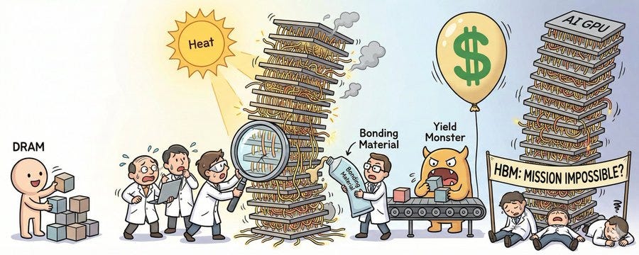
HBM is everywhere in the conversation right now. Stock forums, news outlets, casual dinner tables — everyone’s heard that “HBM is in short supply” or “NVIDIA can’t build enough GPUs because of HBM.”
But almost nobody explains why it’s actually hard. Most coverage stops at “they stack dies using TSVs” or “the micro bumps have to align perfectly.” That’s not an explanation. That’s a caption.
This piece walks through every stage of HBM production — design, fabrication, test, packaging — and explains what makes each one genuinely difficult. It also covers what happens after the product ships to a customer, because that’s where things get interesting in ways most people don’t expect. Everything here is based on direct experience and publicly available technical information.
Substack is currently in a trial phase, so all premium quality articles are available for free for now. Once paid subscriptions are introduced, pricing will be set at a level comparable to professional tech writers on Substack. Early supporters will have the benefit of locking in their current pledge price for future paid access.
1. Design: It’s Not Just Stacked DRAM
The bus width problem
A standard DDR5 interface is 64 bits wide. HBM3E runs at 1,024 bits. HBM4 pushes that to 2,048 bits. Wider bus doesn’t just mean more wires — every I/O pin needs its own signal path, and once you account for power and control signals, a single HBM3E or HBM4 stack requires over a thousand connections to the GPU sitting next to it.
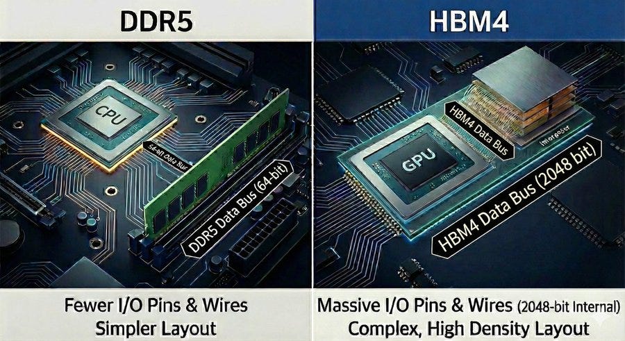
You cannot route that over a PCB. The geometry doesn’t work. That’s the fundamental reason silicon interposers exist, and why 2.5D packaging like CoWoS is non-negotiable. We’ll come back to that.
Power distribution through TSVs
One of the most underappreciated design challenges in HBM is the Power Distribution Network. Delivering clean power through TSVs across 12 or 16 stacked dies is genuinely difficult — during high-current events like refresh operations, voltage droops become a serious problem at the upper dies.
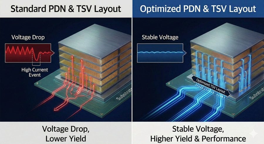
How a company arranges its TSV layout to manage this is one of the core proprietary differentiators between memory vendors. It directly determines yield and performance, which is why nobody publishes it.
HBM4’s logic base die
HBM4 changes the rules. Previous generations used DRAM process technology throughout. HBM4’s base die — the bottom layer of the stack — will be fabricated on a foundry-class logic process, with TSMC 12nm and Samsung’s SF-class node cited in industry reports. Confirmed node specifics are still pending official announcements from each company.
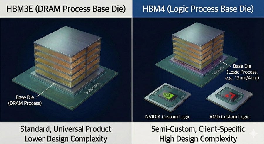
More importantly, this base die can carry customer-specific logic. That means NVIDIA’s HBM4 and AMD’s HBM4 will be physically different products. Memory is transitioning from a commodity component to a semi-custom one, and for the memory vendors, the design complexity that comes with that is enormous.
2. Fabrication: Yield Is the Whole Game
TSV formation
A TSV is a vertical hole etched through a silicon wafer and filled with copper. The diameter is just a few micrometers, and the aspect ratio — depth relative to width — is high enough that both the etch and the plating steps are prone to defects.
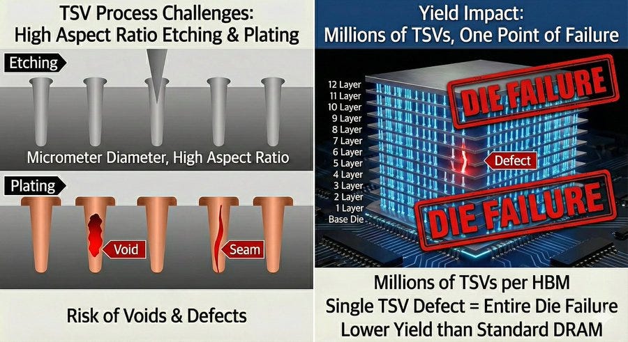
A 12-layer HBM stack contains millions of TSVs. One bad connection means a dead die. TSV yield is substantially harder to control than conventional DRAM fabrication, which is why HBM vendors build TSV repair schemes into their designs to limit the damage from individual failures.
Wafer thinning
To stack dies, each wafer has to be ground down to an extreme thinness. A 12-layer HBM requires dies at around 50 micrometers. Going to 16 layers means getting down to 30 micrometers — less than half the thickness of a human hair.
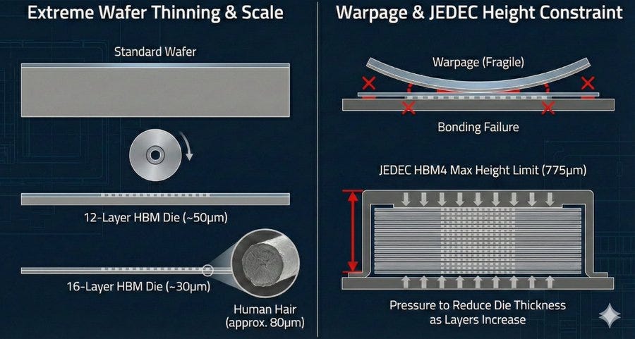
At that thickness, wafers crack easily and bow under their own stress. A bowed wafer cannot be bonded with the precision HBM requires. JEDEC package height constraints tighten further with each generation, so the pressure to thin each die only increases as layer counts go up. The 775 micrometer figure cited in some HBM4 discussions reflects draft specifications, not yet a finalized JEDEC standard.
HBM consumes far more wafer capacity than standard DRAM
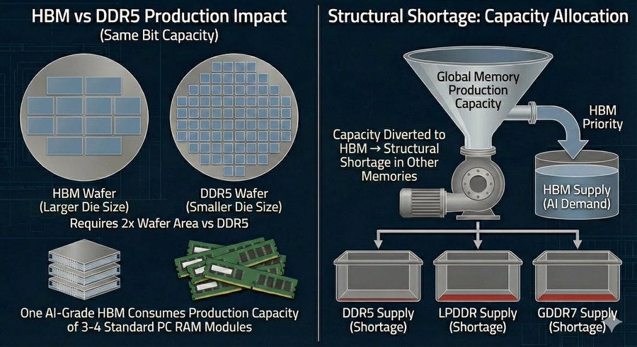
On a bit-for-bit basis, HBM consumes roughly two to three times the wafer area of conventional DRAM. This is an industry estimate based on die size and process overhead, not a precise published figure — but the directional implication is real. When fabs allocate capacity to HBM, DDR5, LPDDR, and GDDR7 all get squeezed. The current tightness in those markets is a structural consequence of that tradeoff, not bad planning.
3. Test: Hard Before Stacking, Harder After
Wafer-level burn-in
Once DRAM wafers come out of fab, the first step is burn-in — running the dies at elevated temperature and voltage to screen out early-life failures. This is followed by functional testing at both low and high speeds. So far, this is similar to standard DRAM production. The hard part starts next.
KGD: the gate you can’t skip
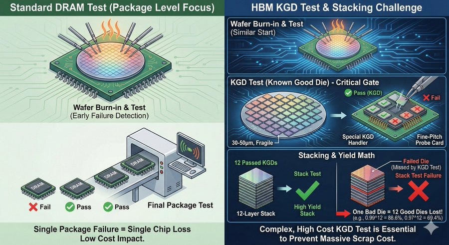
Standard DRAM fails at the individual package level. One bad die, one scrapped unit. HBM is different. Because you’re stacking 12 dies together, every single die has to be confirmed good before assembly. This is called Known Good Die testing, and the math behind it explains why it matters so much.
Assume individual die yield is 99%. For a single chip, that’s fine. Stack 12 of them and the probability that all 12 are good drops to 88.6%. Drop per-die yield to 97% and a 12-layer stack comes out at 69.4% yield. Every bad die in the stack takes down all the good ones around it. That cost structure is what makes KGD testing worth the investment.
The testing itself isn’t straightforward either. Post-dicing dies are 30 to 50 micrometers thick — fragile enough to crack under the wrong handling. Dedicated die-level handlers are required. Probe card pitches shrink with every generation, and a single setup can cost tens of millions of won. The tradeoff between test coverage and test time has real consequences in both directions: too little coverage and defects make it into the stack, too much and throughput collapses.
Post-stack test
After the dies are stacked and connected through TSVs, an entirely new set of problems appears. Verifying bond alignment and interconnect integrity becomes exponentially harder as layer count increases. Isolating a defect to a specific die, bank, and row in a 12-layer stack — based entirely on external test access — is exactly as difficult as it sounds.
Final package test adds at-speed functional testing on top of that, and many vendors now run both ATE and System Level Test in sequence. The cost of finding a defect after full assembly justifies the redundancy.
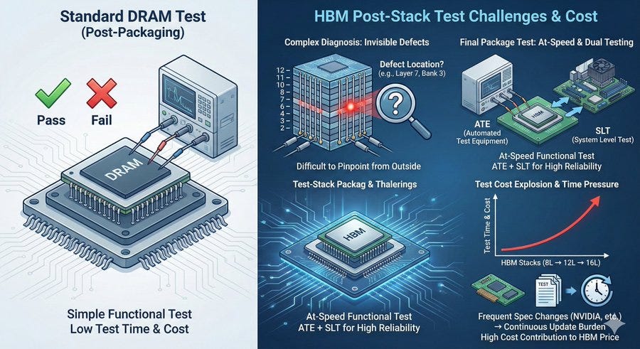
Test infrastructure falls behind product cycles
Moving from 8 layers to 12 to 16 increases test time proportionally. But HBM generations turn over faster than conventional DRAM. Test program development, probe card design, and BIST IP updates all have to land in time for product launch. When a customer like NVIDIA revises its interface specifications, the test conditions have to be rebuilt from scratch. That infrastructure burden has pushed test cost to a significant portion of total HBM manufacturing cost.
4. Packaging: The Most Precise Assembly in Semiconductor History
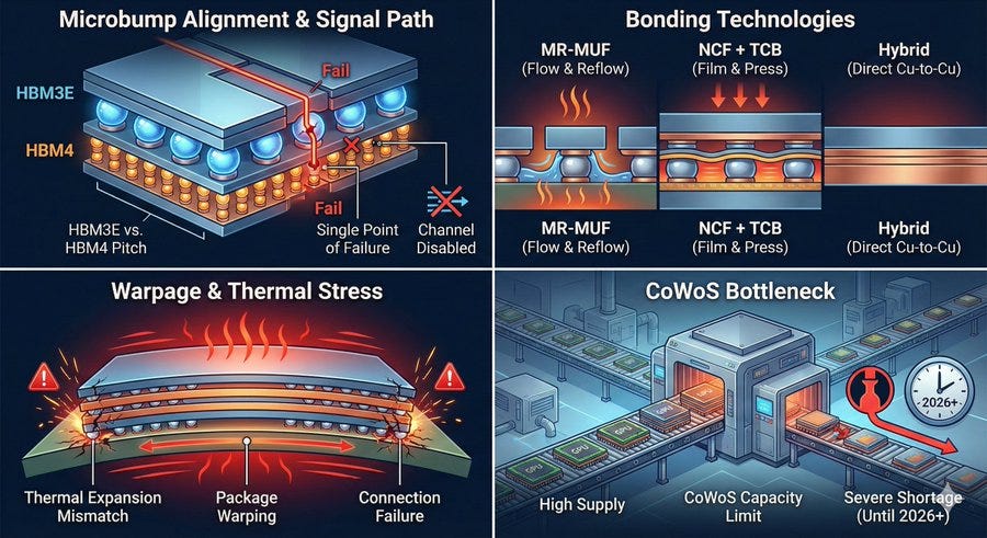
Microbump alignment
Dies are connected layer to layer through microbumps. HBM3E runs at a bump pitch of around 25 micrometers. HBM4 at 16 layers is expected to push that down to 16 to 18 micrometers.
If a bump misaligns, the connection fails. There is no bump-to-bump rerouting redundancy in the HBM PHY signal path — each signal maps to exactly one bump. If that bump fails, the entire channel it serves goes down. HBM3E has eight channels, so a single bump failure doesn’t immediately kill the whole stack, but a dead channel means reduced bandwidth, and in a data center workload context, a GPU running at partial memory bandwidth is effectively unusable.
MR-MUF vs. NCF vs. hybrid bonding
SK Hynix uses MR-MUF (Mass Reflow Molded Underfill), which offers strong thermal performance and is currently the most production-proven approach. Samsung uses NCF (Non-Conductive Film) with thermocompression bonding, which provides better precision at fine pitches.
The longer-term direction is hybrid bonding, which eliminates bumps entirely. It’s already in production for stacked CMOS image sensors. The challenge for HBM is the combination of TSV integration and layer count — applying hybrid bonding across 12 or more layers introduces new yield, metrology, and long-term reliability questions that remain unsolved at production scale.
Warpage
As layers stack up, the accumulated mismatch in coefficient of thermal expansion between dies builds mechanical stress throughout the package. The result is warpage — a bow in the package that compounds with every additional layer. Simulation data consistently shows increasing residual stress as layer count grows, and that stress affects both downstream assembly and field reliability.
CoWoS: the bottleneck that outlasts the die
Finishing the HBM stack is not the end of the line. The HBM still has to be integrated with a GPU or ASIC on a silicon interposer through TSMC’s CoWoS process. As of now, TSMC’s CoWoS capacity is sold out through 2026. That single constraint is the narrowest point in the entire AI chip supply chain.
5. After Delivery: Shipping It Doesn’t Mean You’re Done
HBM ships to customers — NVIDIA, AMD, Google and others — as a standalone component. The customer assembles it alongside their GPU or ASIC into a 2.5D SiP. That’s where a new set of problems begins.
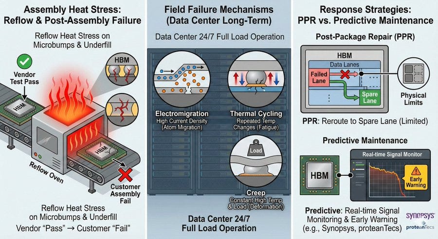
Thermal stress during customer assembly
The customer’s packaging process involves reflow heat treatment, which puts additional thermal stress on the microbumps and underfill inside the HBM stack. Parts that passed every test at the memory vendor’s facility can develop problems after going through the customer’s assembly line. It happens.
Three failure mechanisms in the field
In data centers running 24/7 at full load, three degradation mechanisms work in parallel. Electromigration moves metal atoms along fine interconnects under sustained high current density. Thermal cycling fatigues interconnects through repeated temperature swings. Creep deforms solder joints under prolonged high-temperature mechanical load. A product that passed qualification marginally — not with strong margin, just enough to pass — can fail quietly in the field months or years after shipment.
PPR and predictive maintenance
The HBM specification includes Post Package Repair, which allows a failed lane to be replaced with a spare. It works when the defect is isolated and the spare budget hasn’t been exhausted. For physical damage that has accumulated over time, hardware replacement is ultimately the only answer.
That limitation is pushing the industry toward predictive maintenance — continuous monitoring of signal quality during normal operation, so degradation can be detected before it turns into a system failure. Synopsys and proteanTecs are among the companies building solutions in this space.
What this actually looks like — from my time at AMD
I dealt with this firsthand at AMD. When an HBM-related failure surfaces at the product level, you immediately run into three walls.
The first is attribution. Is this an HBM failure or a GPU failure? Since both are integrated into the same package, there’s no way to probe internally. You’re working from symptoms and trying to reason backward to a cause.
The second is test methodology. Even once you’ve narrowed it to HBM, you have to figure out how to retest it at the system level. The test environment a memory vendor uses before shipment and the environment a customer can access on a finished SiP are completely different. There’s no pre-existing playbook. You build the methodology from scratch, under schedule pressure.
The third is the vendor interface. Getting useful analysis from the memory vendor requires giving them the right data in a format they can actually work with. That interface — what information to share, in what structure — is rarely established in advance. And the vendors’ own field support capacity is limited. When something goes wrong in production, the engineers who can actually help are already stretched thin. The result is that field failures at this level generate a disproportionate amount of wasted time and resources on both sides.
The Bottom Line: Why HBM Is Expensive and Why It’s Scarce
If there’s one sentence that captures why HBM is so hard, it’s this: it’s the only product in the semiconductor value chain where every single stage is running at maximum difficulty at the same time.
And even after clearing all of that to actually produce HBM, you still have to go through CoWoS packaging to get to a finished product — and that line is sold out through 2026.
That’s why HBM is expensive, why it’s scarce, and why memory company stock prices keep going up.
It’s difficult
Great article Damnang. I read your series on POET and all of the accompanying articles on the Photonics Market and the major players in it. Honestly, that was a masterclass in explaining the different technologies, standards and who MAY be the winners in the next few years. It may be a big ask, but as I start reading your post on HBM4, I think a similar series on the Memory Market and how each of the major players (Samsung, SK Hynix, MU, SNDK) standout and who has the edge would be a great read for all of your followers. The most interesting company to me is actually RMBS, whose IP is everywhere and is I feel not as well understood by the market. Your thoughts would be appreciated. Thanks again for all your great work!!