


Since publishing the Optical Investment Map, I’ve heard from a lot of readers. The common thread: the optical theme has already run up significantly, and it was hard to know which names to look at or how to approach them. The investment map helped by laying out the full value chain and the competitive dynamics at each layer. What I found most rewarding was hearing that people used it not just to pick individual stocks, but to build their own investment strategy and portfolio.
Damnang's Optical Investment Map v1.0

These days the market is drowning in words like optical, silicon photonics, and CPO. But most investors know the keywords without actually seeing the full picture of the value chain behind them.
But if you look closely at that map, there was one layer among the seven that clearly stood apart.
Layer 7: Test.
Layers 1 through 6 are fundamentally about making and moving light. You lay down materials, build lasers, design PICs, package them, and assemble modules. Each layer connects naturally to the ones above and below.
Test is different. Test sits outside this flow and cuts across every stage. You need testing at the wafer level, the package level, and the system level. The customers are different, the cycles are different, and the competitive landscape is different. It’s far too broad and deep to compress into a few lines within a single layer.
As an engineer who studied semiconductor test and works in Silicon Valley doing test and silicon debug, I’m convinced that optical test, specifically CPO test, is the area that demands attention right now. As optics move inside the package, the complexity and cost of test are structurally changing. And this shift is not yet fully reflected in the market.
In this article, I’m pulling Layer 7 out of the Optical Investment Map and analyzing it separately. The point is not simply to list test equipment companies. It’s to work through which bottlenecks open first under different CPO adoption scenarios, and which companies can capture the economics of those bottlenecks.
To do this, I break the optical test value chain into 5 bottlenecks and evaluate 14 stocks across 6 investment Factors. This is not a single ranking. The stocks you should watch change depending on which CPO scenario you believe in.
Disclaimer
This article is based on publicly available information and general industry knowledge. It does not contain any NDA-protected or confidential information from any company, and is not a buy or sell recommendation.
Why CPO Test Matters Right Now
The direction of optical interconnects is already set. The path goes from pluggable to NPO, and ultimately to CPO. The closer the optical engine moves to the ASIC, the better the power efficiency and bandwidth density.
As of 2026, 800G pluggables are in high volume and 1.6T is ramping. Up through this stage, existing test infrastructure can handle the workload. You test the ASIC on its own, and the module maker tests the optical module separately.


But CPO is a different game.
When the PIC moves inside the ASIC package, the economics of test change. With pluggables, if you get a bad optical module, you pull it out and swap it. But in CPO, the PIC, EIC, and switch ASIC are bonded together inside a single package. If a PIC defect is discovered late, you may have to scrap the entire expensive ASIC package. That’s why securing Known Good Die from the PIC before packaging becomes a critical prerequisite for CPO mass production.
This shift matters for test equipment companies for three reasons.
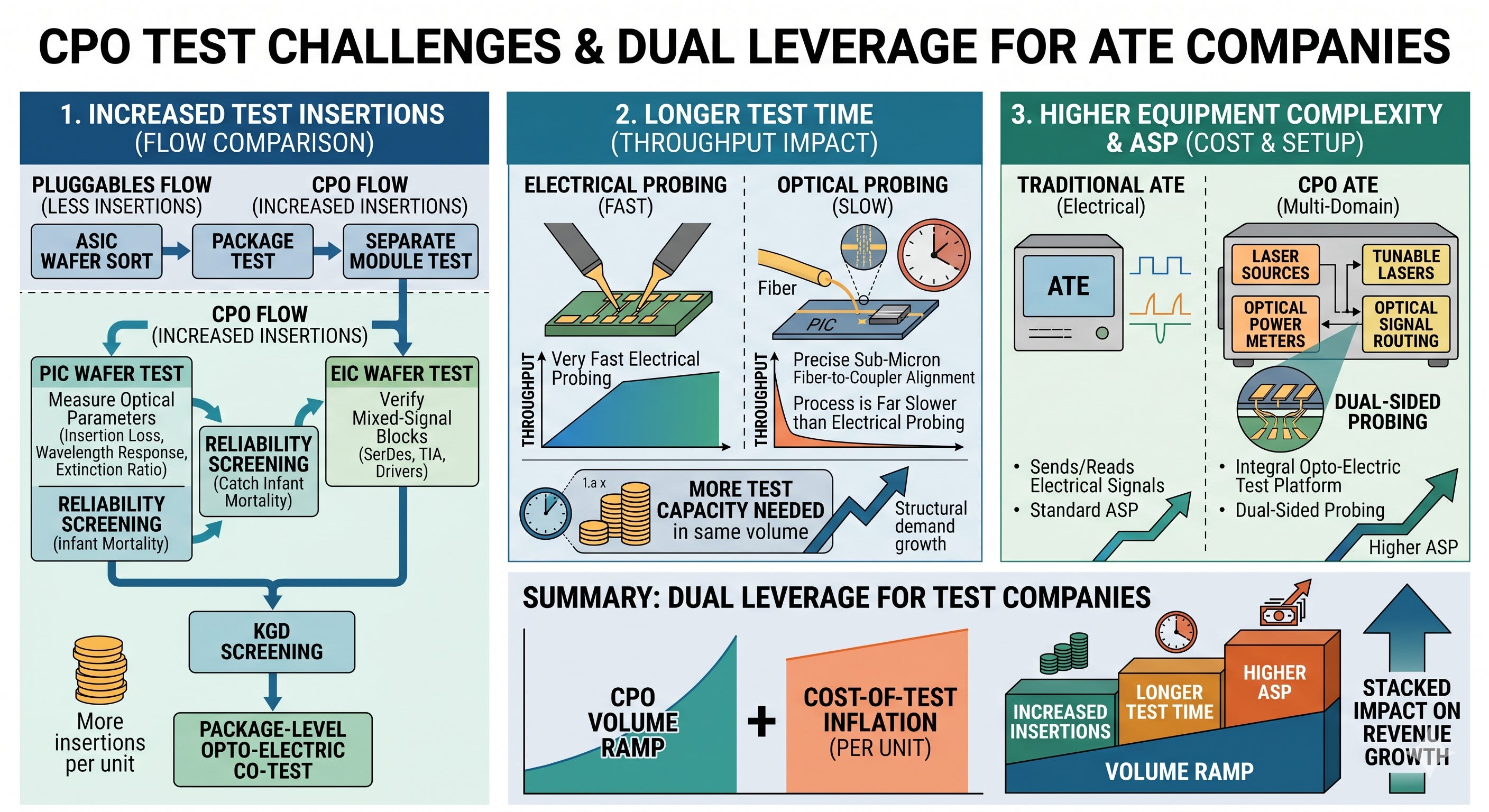
First, test insertions increase. With pluggables, you could separate the flow into ASIC wafer sort and package test, plus a separate module test. CPO requires PIC wafer test, EIC wafer test, KGD screening, and package-level opto-electric co-test.
PIC wafer test means measuring optical parameters like insertion loss, wavelength response, and modulator extinction ratio. On the EIC side, you need to verify mixed-signal blocks like SerDes, TIA, and drivers. On top of that, you add reliability screening to catch PIC infant mortality before packaging.
Second, test time gets longer. Electrical probing is very fast. But optical probing of a PIC requires precisely aligning a fiber to the coupler. Sub-micron alignment is needed, and this process is far slower than electrical probing. When throughput drops, you need more test capacity to process the same wafer volume. This is why test equipment demand can grow structurally even without an explosion in volume.
Third, equipment complexity and ASP go up. Traditional ATE sends and reads electrical signals. CPO requires integrating laser sources, tunable lasers, optical power meters, and optical signal routing into the test setup. Some architectures even require dual-sided probing, with electrical pads accessed from the top and optical couplers from the bottom. At that point, this is no longer a matter of bolting a few optical modules onto existing ATE. The test platform, probe interface, optical measurement, and automation flow all need to change.
The net result is that CPO creates dual leverage for test companies. It’s not just about CPO volume growing. The number of test insertions per unit increases, test time per unit gets longer, and equipment ASP goes up. You get per-unit cost-of-test inflation stacked on top of volume ramp.
This market has not yet hit a full-scale production explosion. That distinction matters. What’s opening right now is not the CPO volume market, but the CPO test infrastructure cycle. TSMC’s COUPE platform has been reported to be entering volume production in 2026, and Samsung Foundry has declared a CPO turnkey target for 2029.
NVIDIA announced Spectrum X and Quantum X photonics switches, officially committing to the photonic networking direction. As PIC wafers start coming out of foundries and CPO package flows take shape, the very first question is: what equipment, at what precision, and at what cost structure will be used to validate those PICs and packages?
That’s why equipment companies are moving first. Teradyne launched Photon 100 and acquired Quantifi Photonics. FormFactor acquired Keystone Photonics and is pushing the Triton test cell alongside Advantest and Tokyo Electron. Aehr has won SiPh WLBI customers and is positioning on the silicon photonics reliability side. Viavi, Santec, and Anritsu are all aligning their products and messaging toward 1.6T, 3.2T, and silicon photonics test.
In other words, this is not the point where CPO has already been deployed at scale. This is the point where equipment companies are shipping products, customer qualifications are starting, and early orders and design wins are accumulating. Actual large-scale deployment is likely post-2028. That’s exactly why the investment thesis right now is less about a CPO volume bet and more about an early-cycle bet on CPO test infrastructure getting built out.
Market perception has not fully caught up to this shift. Many investors still see Teradyne as a memory and SoC ATE company, Viavi as a telecom T&M company, and Aehr as a small-cap SiC burn-in name. But if CPO test opens up, the growth narrative for these companies could change meaningfully.
The customer structure is also different from the traditional ATE market. The usual semiconductor test customers are IDMs, foundries, and OSATs.
In optical test, module makers and hyperscalers enter the picture. It’s not just Coherent, Lumentum, and Innolight; hyperscalers who are directly architecting their own optical interconnects also influence the test ecosystem.
The cycle is different too. SoC ATE demand is tied to GPU and ASIC ramps, but optical test demand moves with the pace of pluggable-to-NPO-to-CPO transitions. This timing can be offset from the traditional semiconductor test cycle by one to two years.
That’s why I don’t view optical test as a small subcategory of the existing ATE market. As CPO scales, test becomes its own investment cycle.
And that cycle is still in its early stages.
5 Bottlenecks in CPO Test
I’m re-dividing Layer 7 of the Optical Investment Map into 5 bottlenecks. This is not a simple equipment classification. The more important questions are:
Where does yield get stuck in the CPO production process? Where does test cost escalate? And which companies can convert that cost increase into revenue?
Even within the same bottleneck, the investment character is completely different depending on the company. Some companies move at the front end of the CPO capex cycle, while others span both pluggable and CPO. Some are tied to wafer-level KGD, others to packaging yield and reliability.
So the first step is to map where money gets stuck within the CPO test value chain. Picking good companies comes after that.
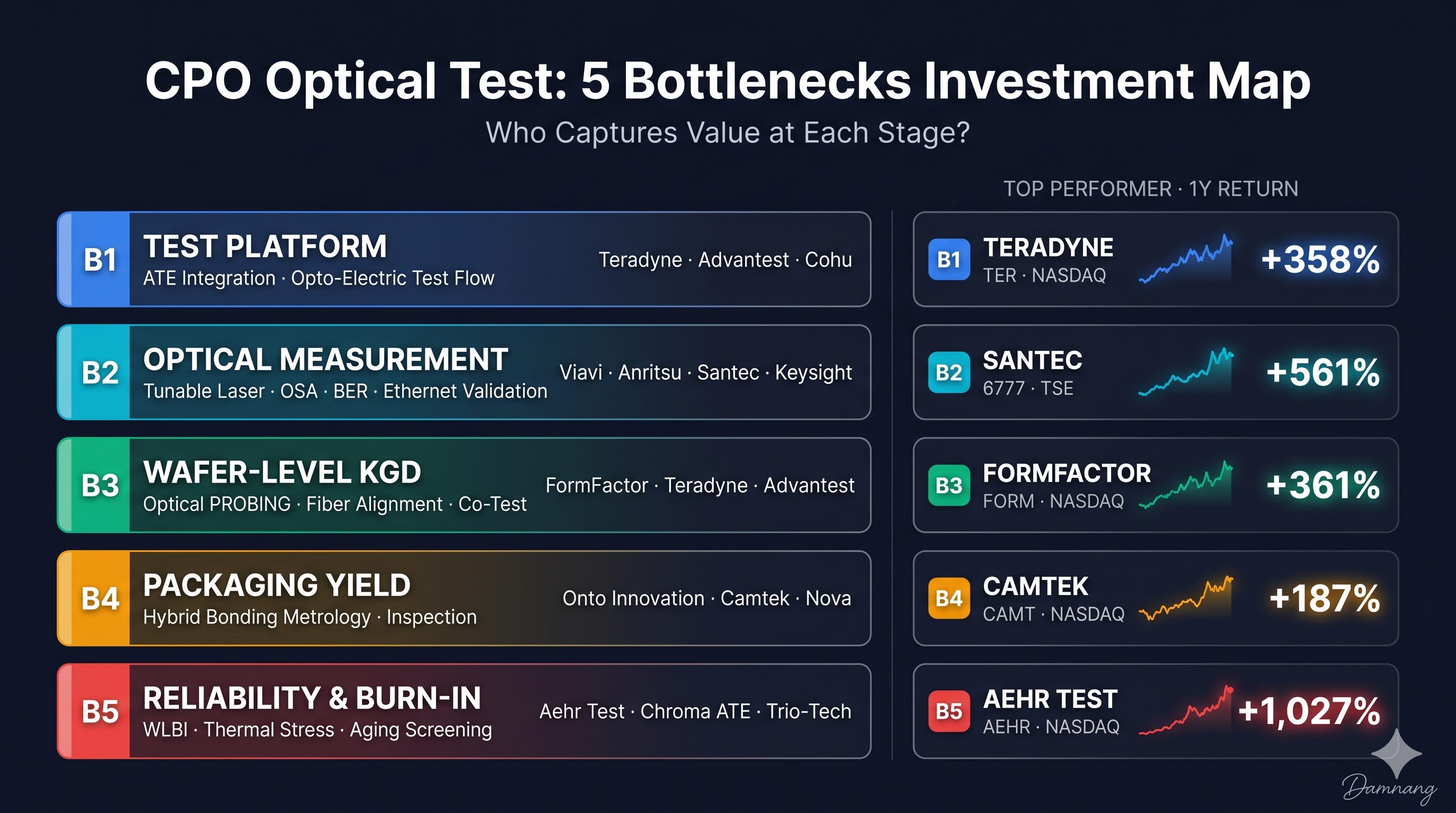
Bottleneck 1: Test Platform
Can CPO test be integrated into the existing electrical ATE flow?
In CPO, you cannot separate electrical and optical signals. At the wafer level, the optical engine level, the package level, and the module level, electrical test and optical test need to live within the same flow. So this is not about adding one piece of equipment. The test OS, handler, automation, test cell, and software flow all matter.
This bottleneck sits at the front end of the CPO infrastructure cycle. When foundries, OSATs, and hyperscalers prepare CPO lines or pilot production, the first thing they need is a production-ready test platform. That makes this the area most likely to generate revenue first when CPO capex opens up.
That said, this space is already dominated by large ATE incumbents. Companies like Teradyne and Advantest hold strong positions in SoC and memory test and are already capturing some AI test premium. CPO upside is real, but until CPO-specific revenue is visibly broken out, valuation risk needs to be weighed alongside it.
Relevant stocks: Teradyne (Photon 100, Quantifi Photonics acquisition, vertical integration strategy), Advantest (V93000-based open ecosystem), Cohu (supplementary exposure via handler, thermal, and automation)
Bottleneck 2: Optical Measurement
How fast and accurately can you generate, read, and analyze optical signals?
This includes tunable lasers, optical spectrum analyzers, BER testers, optical power meters, and Ethernet validation equipment. This bottleneck is not tied exclusively to CPO. It remains relevant across the 800G pluggable, 1.6T, and 3.2T optical transceiver cycle.
That makes Optical Measurement the most defensive bottleneck on this map. Even if CPO is delayed, revenue can hold up as long as optical data center speed upgrades continue. Conversely, if CPO accelerates, demand extends into SiPh wafer test, optical engine test, and package-level optical validation.
From an investment perspective, this is the area that reduces CPO timing risk. However, purity varies significantly by company. Santec has the highest optical test purity but carries valuation risk, Keysight has strong technical capabilities but optical exposure is diluted within the broader company, and Viavi sits in between as the most balanced candidate.
Relevant stocks: Viavi (optical production test and high-speed Ethernet validation), Anritsu (BERTWave-centric optical transceiver test), Santec (tunable laser and optical test pure-play character), Keysight (silicon photonics test system and broad T&M portfolio)
Bottleneck 3: Wafer-Level KGD
Can you secure Known Good Die at the PIC wafer level?
The scariest problem in CPO is a PIC defect discovered too late. If a PIC has already been integrated into an ASIC package when the problem surfaces, you may have to scrap the entire expensive switch ASIC package because of one bad PIC. That’s why securing optical KGD at the PIC wafer level before packaging becomes critical.
This process requires optical probing, electrical and optical co-test, fiber alignment, and in some cases dual-sided probing. You need to precisely align the fiber to the coupler and measure optical parameters like insertion loss, wavelength response, and modulator behavior at the wafer level.
From an investment perspective, this is the most structurally critical bottleneck for CPO yield. Probe cards and optical probing solutions in particular can take on recurring revenue characteristics as wafer volume grows.
However, this bottleneck doesn’t belong to FormFactor alone. The two ATE companies from Bottleneck 1 are reaching down into the KGD stage. Teradyne is pushing vertical integration from platform to wafer probing through its Photon 100 and dual-sided probing collaboration. Advantest covers optical KGD on top of V93000 through the Triton test cell, co-developed with FormFactor and Tokyo Electron. FormFactor holds an ATE-agnostic position that benefits regardless of which platform wins. That’s the key point.
And KGD has two dimensions: measurement-based screening (”does it meet optical spec?”) and stress-based screening (”will it survive over time?”). The former is this Bottleneck 3. The latter is the burn-in covered in Bottleneck 5. Aehr’s WLBI serves as the final gate in KGD.
Relevant stocks: FormFactor (Pharos optical probe, Keystone Photonics acquisition, Triton test cell, ATE-agnostic), Teradyne (Photon 100 + dual-sided probing for vertical integration from Bottleneck 1 to 3), Advantest (Triton test cell for joint coverage with FormFactor)
Bottleneck 4: Packaging Yield and Bonding Metrology
Can PIC and EIC be reliably integrated inside the package?
This bottleneck is not a test layer that measures optical signals directly. But it is an adjacent bottleneck that drives CPO yield economics. To integrate PIC and EIC through hybrid bonding or advanced packaging flows, you need precise inspection of surface defects, bump alignment, bonding quality, and interconnect defects before and after bonding.
CPO packages are expensive. As more components are bundled together (switch ASIC, PIC, EIC, HBM or other chiplets), package value goes up. When yield loss occurs at this stage, it’s not a single-die problem; it’s a scrap problem for an entire high-value package.
From an investment perspective, these companies make money from the advanced packaging cycle before CPO, and CPO is more like an option layered on top. Onto, Camtek, and Nova already hold strong positions in HBM, 2.5D, 3D packaging, and hybrid bonding metrology. Financial quality is high, but the market does not view them as CPO test pure plays.
Relevant stocks: Onto Innovation (DragonFly G5, EchoScan, advanced packaging metrology), Camtek (Hawk, Eagle G5, surface defect inspection), Nova (WMC platform, dimensional and chemical metrology)
Bottleneck 5: Reliability and Burn-In
Can you screen out laser aging, wavelength drift, and early-life failure before production?
Optical devices behave differently from electrical logic. They are sensitive to time, heat, and optical power stress. Laser output can shift, wavelength can drift, and thermal tuning conditions can change. In CPO, the PIC is inside the package, making field replacement difficult when failures occur.
That’s why the importance of reliability screening rises as CPO approaches mass production. If demand grows for catching PIC early-life failures before packaging, wafer-level burn-in and package-level burn-in equipment gain significant value.
From an investment perspective, this is the most lagging bottleneck but potentially the highest-beta one. As CPO volume production draws closer, reliability and burn-in demand can be rapidly re-rated. Conversely, if CPO ramp is delayed, earnings conversion in this space gets pushed out too. So this area carries large upside and large timing risk simultaneously.
Relevant stocks: Aehr Test Systems (FOX XP-based wafer-level burn-in), Chroma ATE (PIC burn-in and Asian local ecosystem), Trio-Tech (burn-in board and burn-in service exposure)
That covers the structure of the CPO test value chain. The 5 bottlenecks show where yield gets stuck, where cost escalates, and which areas can generate revenue first.
But knowing the bottlenecks and picking stocks are two different things.
Even within the same bottleneck, every company has a completely different profile. Some have high optical purity but already carry elevated expectations in their valuation. Some have deep technical advantages but no clear CPO-related orders yet. Some need CPO to arrive quickly, while others can make money from the pluggable cycle even if CPO is delayed.
So saying “CPO test is heating up” is not enough. What matters is which bottleneck opens first under the CPO adoption timeline you believe in, and which company can actually convert the economics of that bottleneck into revenue.
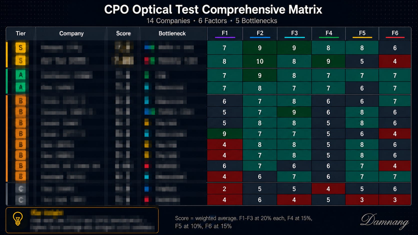
From here, I evaluate the 14 stocks across 6 investment Factors: optical theme exposure, CPO cost-of-test leverage, technical advantages, real orders and catalysts, financial quality, and valuation risk.
Why AEHR Matters Right Now

The economics of early-stage semiconductor failures are changing fast. As AI data centers scale and optical interconnect architectures move from roadmap to reality, burn-in, once a process reserved mainly for high-reliability applications, is back at the center of manufacturing strategy. AI processors, silicon photonics, and advanced packaging are all converging to drive this shift.
Record Earnings, 8% Drop. Is the Market Reading Teradyne Right?

Teradyne posted its largest quarter ever in Q1 2026. Revenue grew 87% year over year. EPS blew past consensus. The CEO said roughly 70% of the quarter’s revenue was tied to AI demand. Look at the numbers and Teradyne reads like a textbook AI infrastructure beneficiary.