As someone with a strong technical interest in Cerebras and WSE-3, the third generation of WSE, the world’s first commercially available wafer scale AI chip, I suddenly became curious. How should yield even be defined for this enormous chip? Is this wafer scale chip really competitive with conventional GPU chips in terms of yield as well? How should it be tested?
These are probably questions shared not only by me, but also by many others interested in Cerebras.
I have spent more than a decade studying and working on test design, fault diagnosis, and yield improvement, including my doctoral studies and my career at several semiconductor companies. In this article, I want to draw on that experience to build scenarios and calculate a WSE yield model, using the WSE specifications and repair methods Cerebras has disclosed so far and the knowledge of testing, yield, and failure analysis I have accumulated in the industry.
Of course, the calculations and numbers in this article are results from assumptions and models I built using public information. They are not Cerebras’s actual yield, and the problem cases may not occur in practice. Applying the actual N5 process conditions and Cerebras’s undisclosed repair techniques and test methodologies could lead to conclusions that differ in many respects from the assumptions in this article. Even so, I wrote this article because I believe it can be a useful guide for general readers without a technical background on how to understand and approach the yield of this unprecedented wafer scale semiconductor chip, the first of its kind in the world.
Cerebras WSE-3: The Technical Achievement and the Physical Ceiling

Cerebras Systems’ WSE-3 hit 2,522 tokens/s per user on Llama 4 Maverick inference. That is more than double the 1,038 tokens/s NVIDIA published for the DGX B200 on the same model.
Disclaimer
This article is for informational purposes and is not a recommendation to buy or sell any specific stock. The author may hold positions in the stocks mentioned, and those positions may change without notice. Readers are responsible for their own investment decisions.
1. Cerebras’s Wafer Scale Chip Can Tolerate Defects
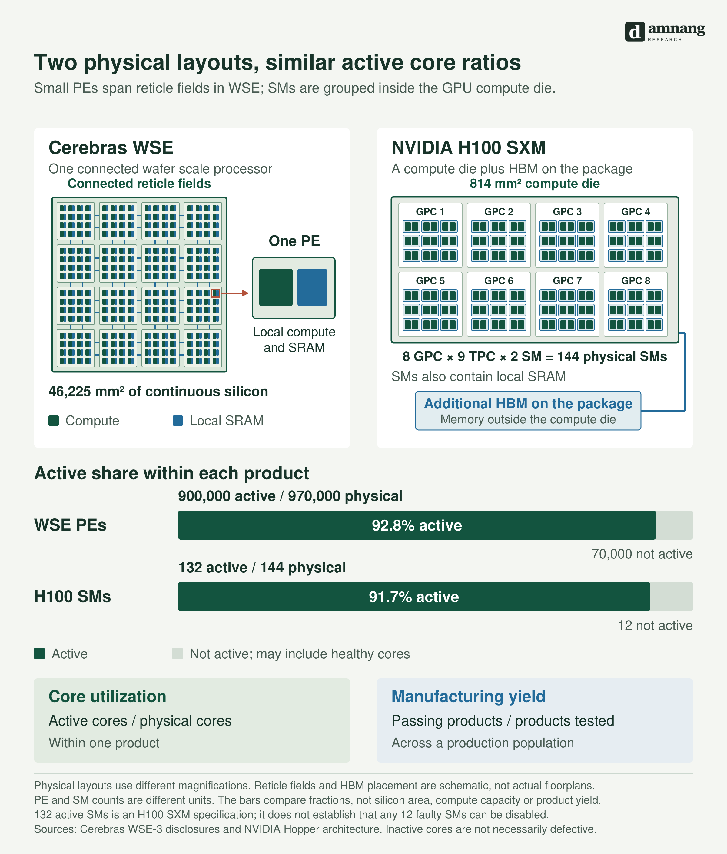
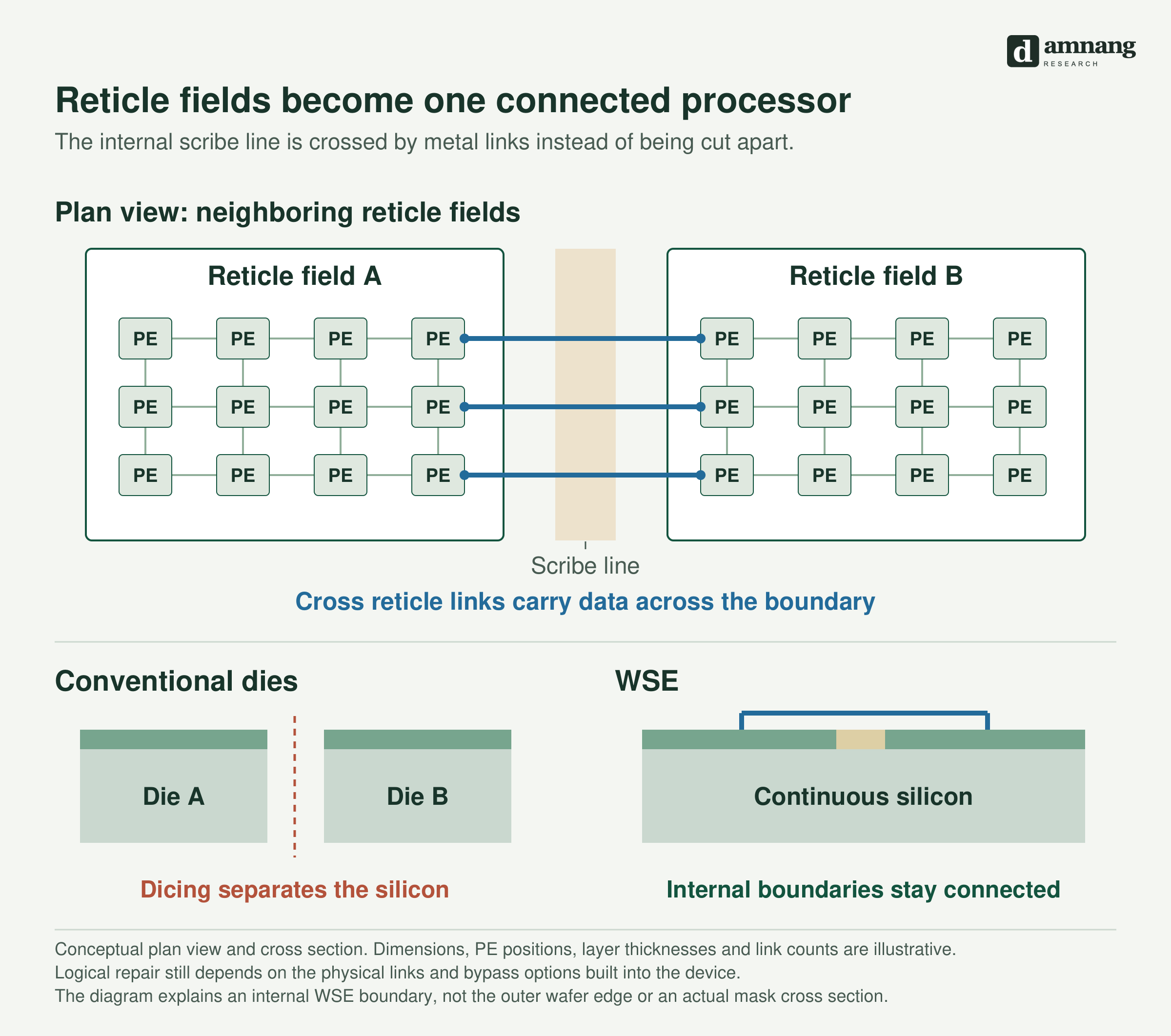
Cerebras’s WSE-3 uses approximately 46,225 mm² of wafer area as a single processor. The small unit that performs computation within it is the PE(Processing Element). Each PE contains a CE (Compute Engine) for computation, Local SRAM for storing data, and a Fabric Router for sending and receiving data.[1] [3] [9]
Each router connects to its neighbors to the north, south, east, and west. This connection is called a Link, and moving along one link to the next router is called a Hop. We call a structure that repeats these connections horizontally and vertically in a 2D mesh a NoC, Network on Chip. Cerebras is known to use this NoC structure.[9]
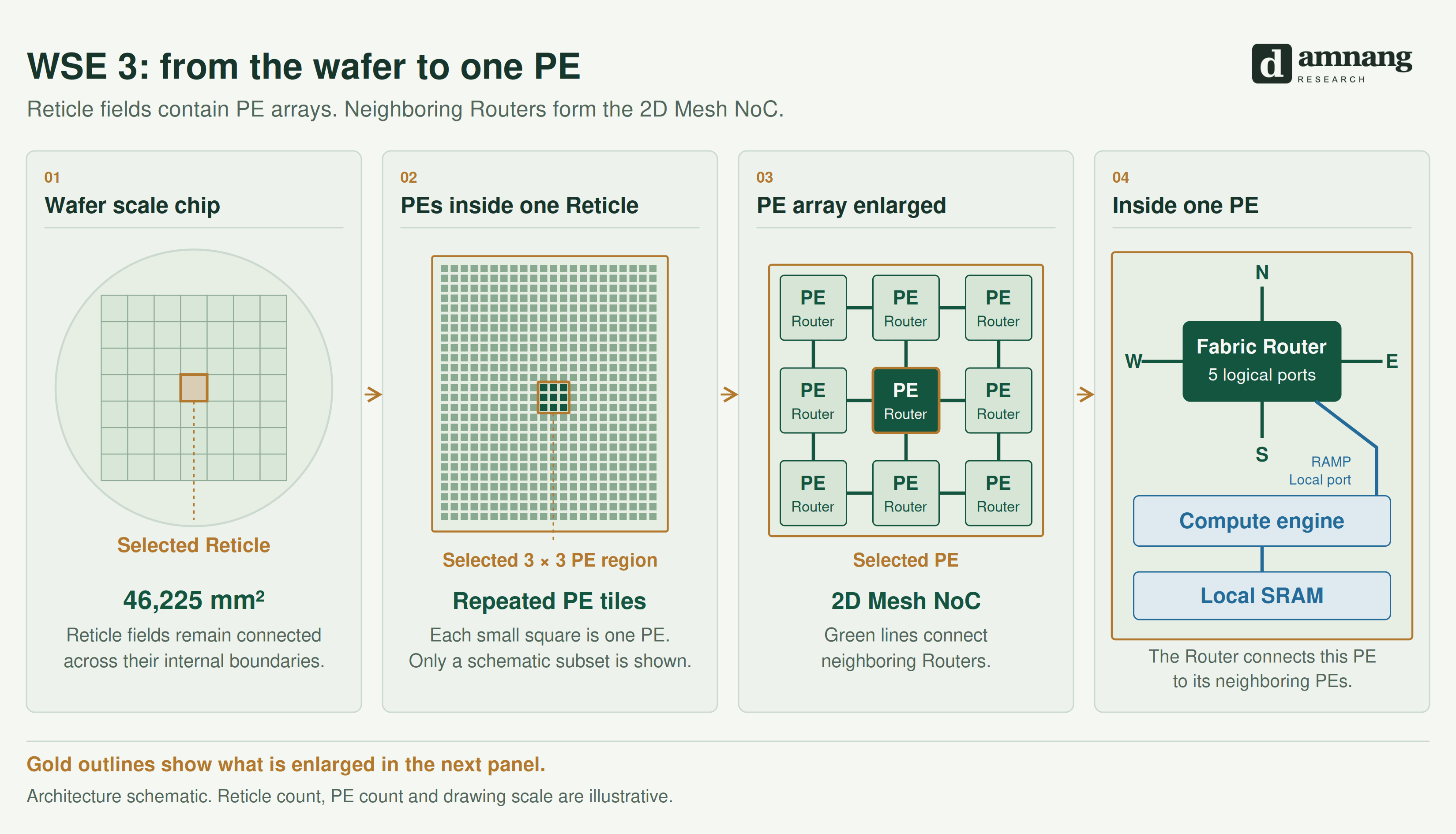
Then what does it mean that this wafer scale chip can tolerate defects?
WSE-3 is reported to contain approximately 970,000 physical PEs. In other words, about 70,000 more PEs are built than the 900,000 required for shipment.
A design that builds more circuitry than needed is described as incorporating Redundancy, logic repair, or fault tolerance. Cerebras has adopted this structure. The idea is to bypass defects instead of discarding the chip when they occur.[1] This structure is possible because AI computation uses many cores with identical functions, and defective cores can be replaced if spare cores and valid connections are available.
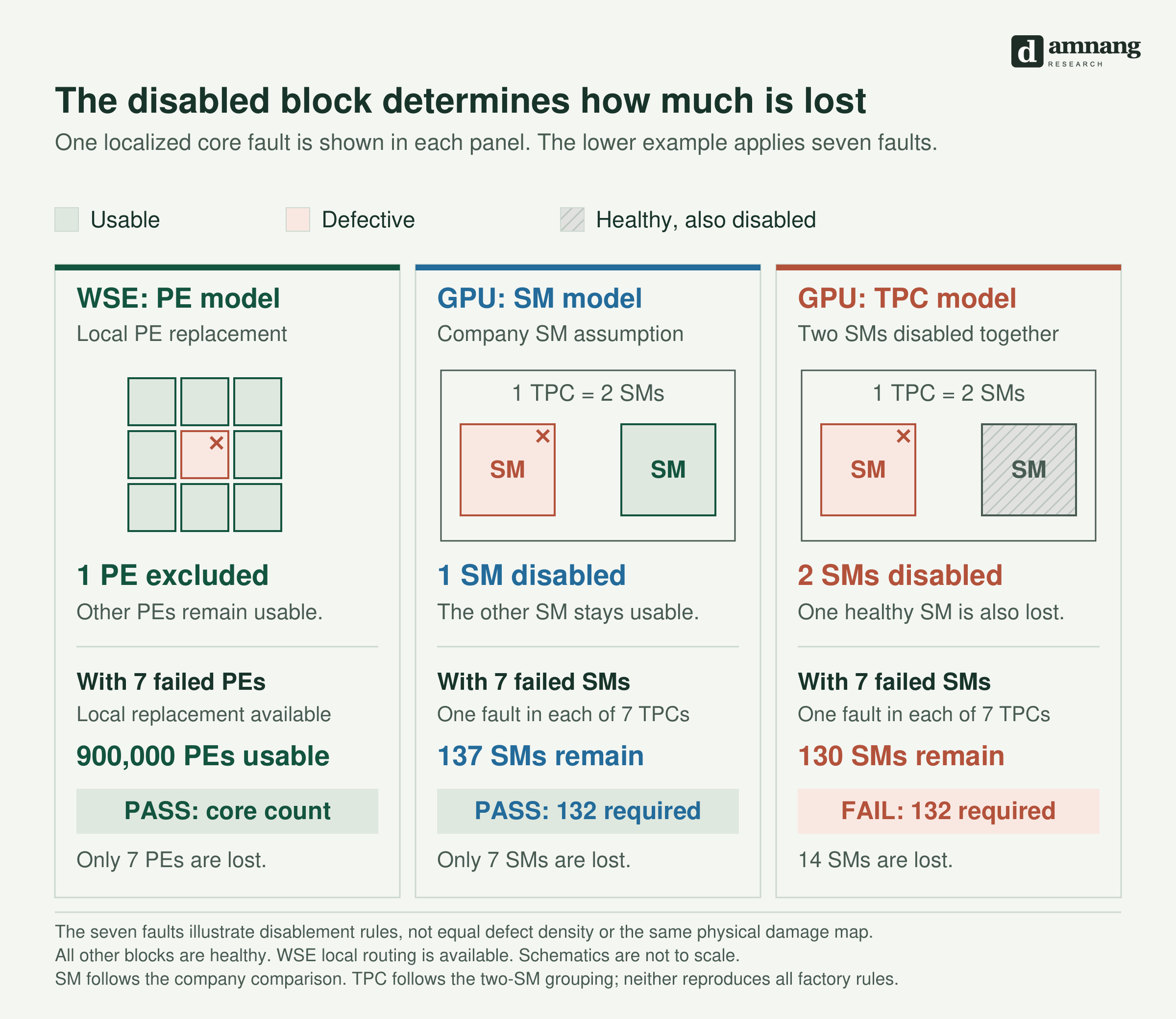
In fact, this is not a new concept. SRAM has long improved yield through memory repair, replacing defective cells with spare rows and columns. The same is true of the conventional GPUs we know. For example, H100 SXM physically contains 144 compute blocks called SMs (Streaming Multiprocessors). Two SMs form one TPC (Texture Processing Cluster), and only 66 of the 72 TPCs are actually used.[4] In other words, GPUs already use a form of fault tolerance.
However, the two structures use different units for shipment qualification. GPUs are judged on whether each die passes, while WSE must secure all the required PEs and connections within a single wafer.
2. Cerebras’s 100x Defect Tolerance Figure Is Really Just a Marketing Number
Cerebras claims that, at the same defect density, a wafer containing 72 dies comparable to H100 loses 361 mm² from about 59 defects, while one WSE-3 loses only 2.2 mm² from about 46 defects. It says this is a difference of 164 times, and that its resulting silicon utilization of 93% is higher than H100’s 91.7%.[1]
Is that really true?
Of course, the numbers from the simple calculation are correct.
But they do not tell us how many wafers out of 100 actually pass. They do not represent actual yield.
To examine this from a yield perspective, I built a random defect model and ran the calculations.
I assumed that defects occur at independent locations and damage only the affected core. I omitted placement constraints within each GPC and defects in shared circuitry, following the same simplification used in Cerebras’s blog.
For the GPU, I used a Floorsweeping model that disables defective TPCs. I assumed a pass if the required 66 TPCs remained after excluding up to six of the 72, and also calculated a supplementary case in which SMs were excluded individually.
I divided WSE into 84 repair regions, allowed up to 833 defective PEs to be replaced per region, and allowed unrestricted connections within each region. 833 is an analytical assumption, not a disclosed actual repair limit.
Note: Both models judge pass or fail only by core count. This is not a comparison using actual yield data from TSMC’s 5 nm process.[4] [5]
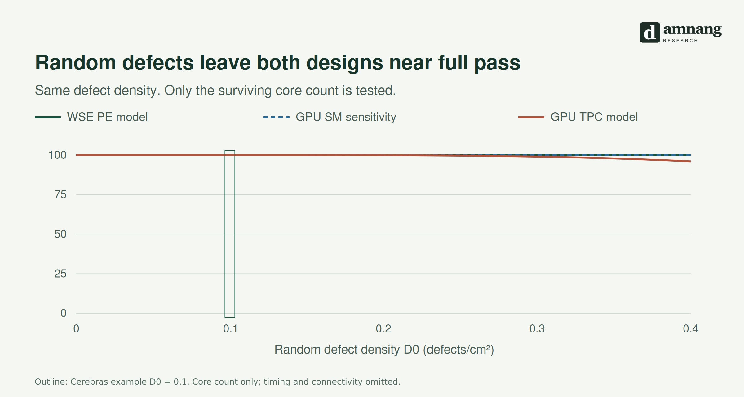
What yield does this defect model produce at D0 = 0.1, the value Cerebras used in its blog?
Regardless of the 164 times figure mentioned in the blog, the calculated results are 99.998% for the GPU TPC model and above 99.999% for the WSE model, which are almost the same. A die fails only if defects affect at least seven TPCs.
At an average of 0.81 defects per die, that occurs in about two out of 100,000 dies.
Next, I calculated the result at D0 = 0.4, four times 0.1, and found an average of 3.3 defects per GPU die. Even under the least favorable assumption, where two SMs are disabled together as a TPC, the GPU model’s pass rate was 96.02%.
If SMs are disabled individually, the rate still exceeds 99.99%. WSE has about 185 defects per wafer, or about 2.2 per region, still far below the limit, so its pass rate exceeds 99.999%.
In other words, the yield gap widened somewhat as D0 increased, but within the range compared, most GPUs also retained the cores required for shipment.
164 times compares the area disabled by defects. It does not mean that shipment yield or the number of defects that can be handled differs by a factor of 164.
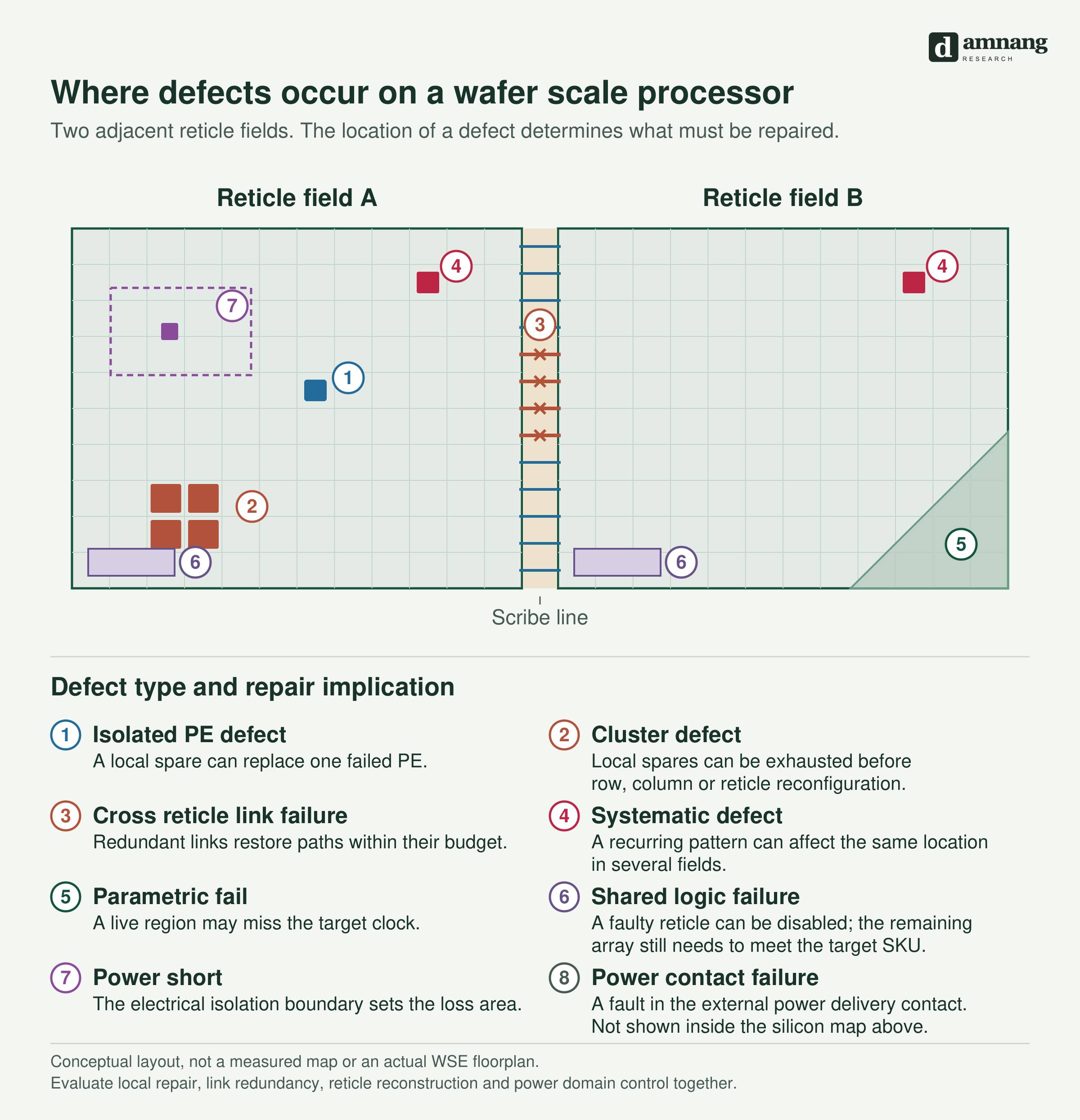
3. Not All Defects Occur in Locations That Are Easy to Repair
In my view, the hardest part of repair (whether for memory or logic) is that defects do not occur in the way I anticipated in the design, and this can make the repair method more complicated.
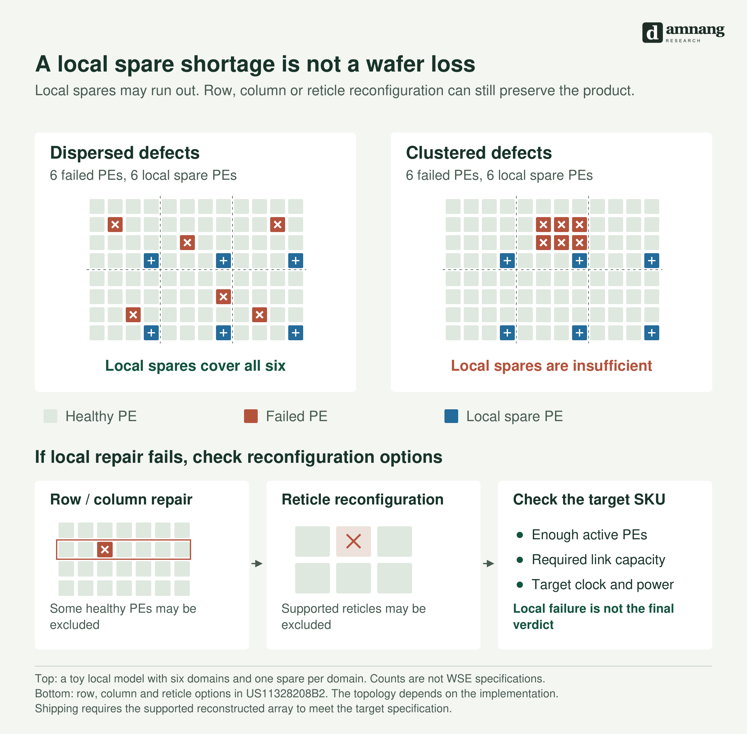
There are many possible defect cases, but one that I think makes repair difficult is the cluster defect model. Defects concentrated in one place may require repair and reconfiguration over a wider area.
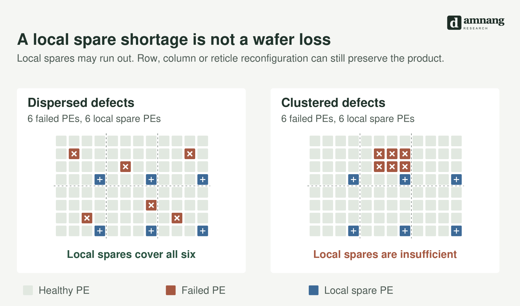
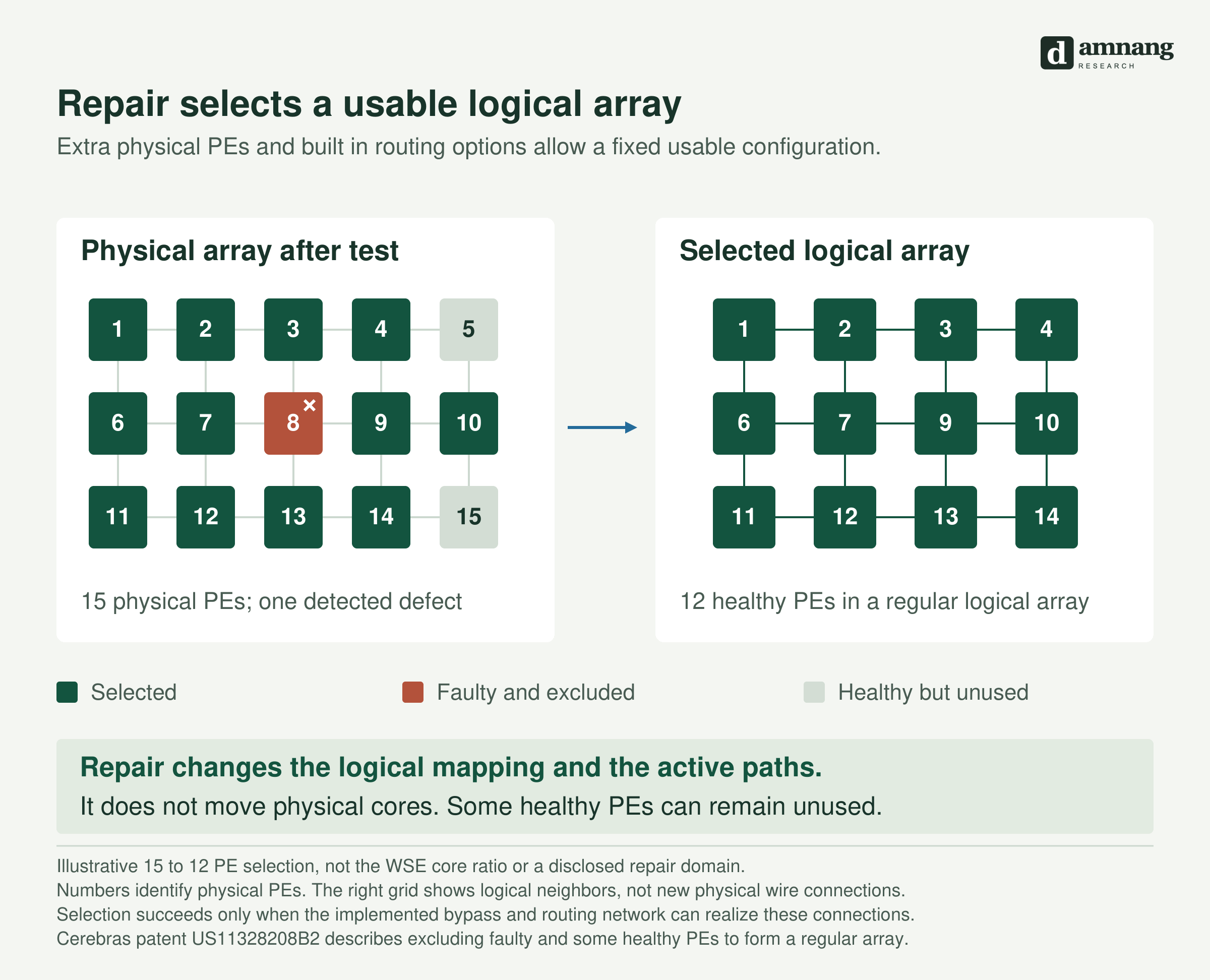
To examine this, I tested a model that selects and connects 45 good PEs out of 63, referring to an example in Cerebras’s patent.[2]
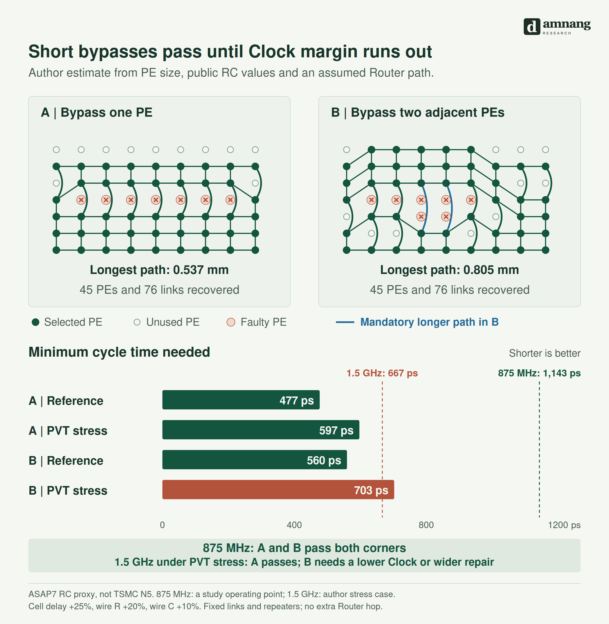
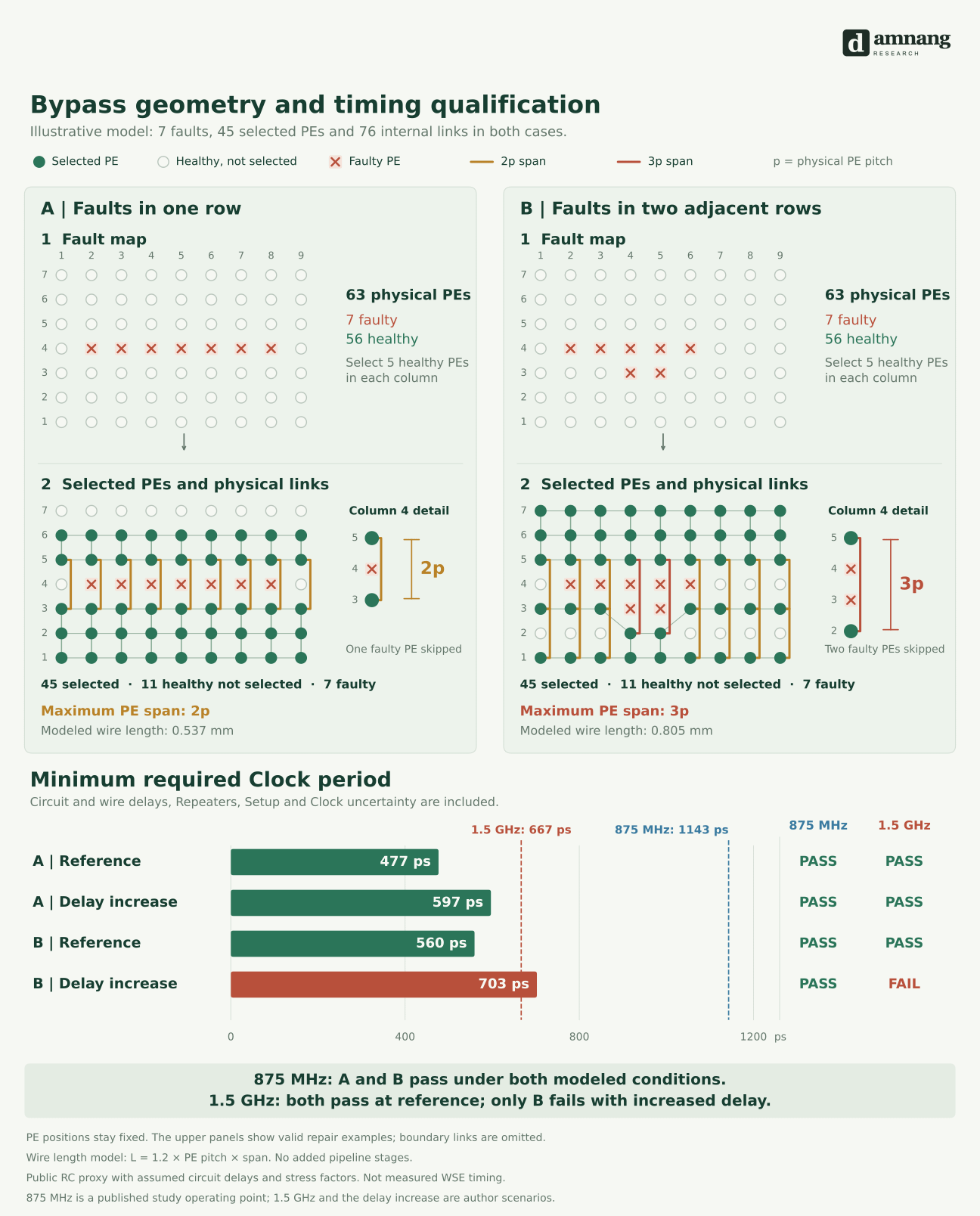
I placed seven defects in both A and B. In A, they were placed in one row. In B, some were placed in two consecutive rows within the same columns. In Figure 4, five good PEs are selected in each column to form a total of 45. A can be repaired with a 2p connection that skips one PE, but columns 4 and 5 of B require 3p connections because two consecutive defective PEs must be excluded. The physical locations of the PEs remain unchanged; only the connection settings change.
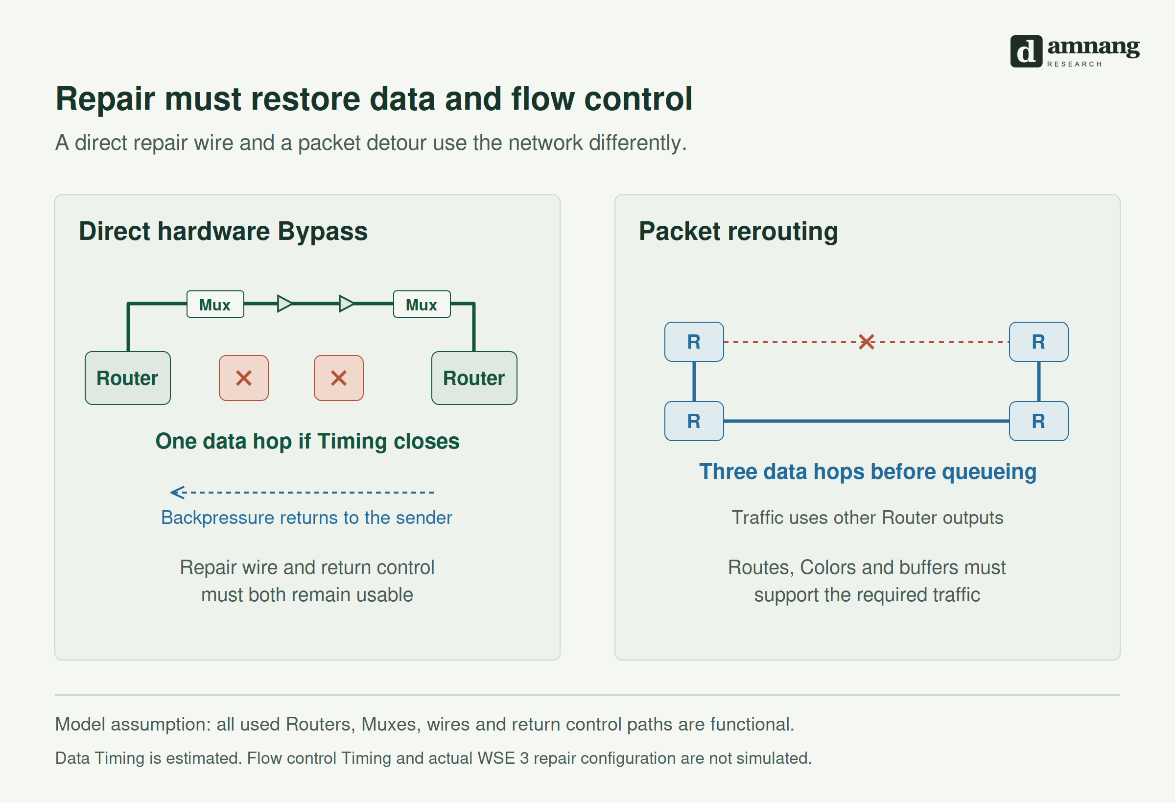
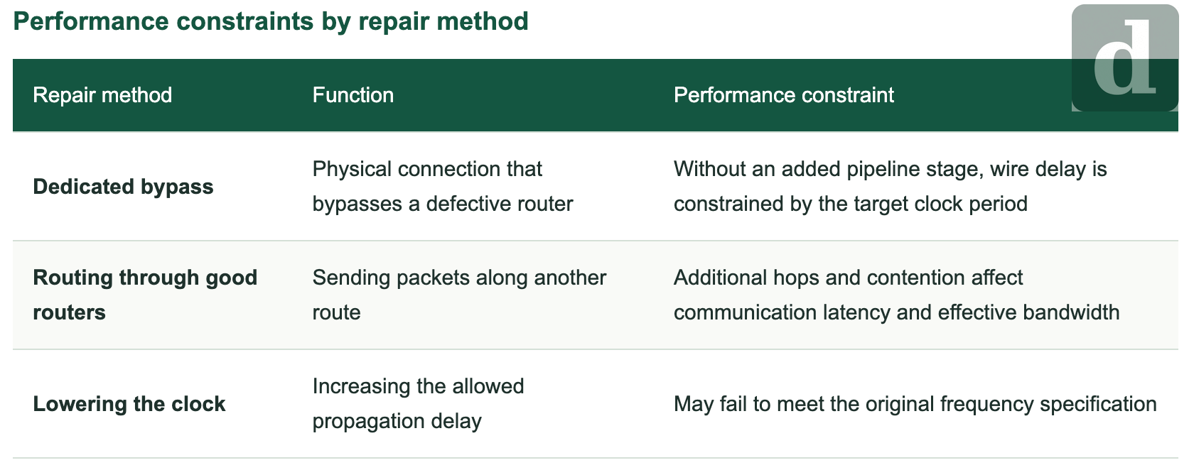
The performance impact of this difference needs to be considered separately for each bypass method. The dedicated bypass in this model is physical wiring that skips intermediate routers. With no additional pipeline stage in between, the signal must cross the long wire within one clock cycle. By contrast, packet rerouting through other good routers can reduce communication performance through additional hops and traffic contention. The delays of these two methods therefore cannot be calculated as if they were the same.[2][9][12]
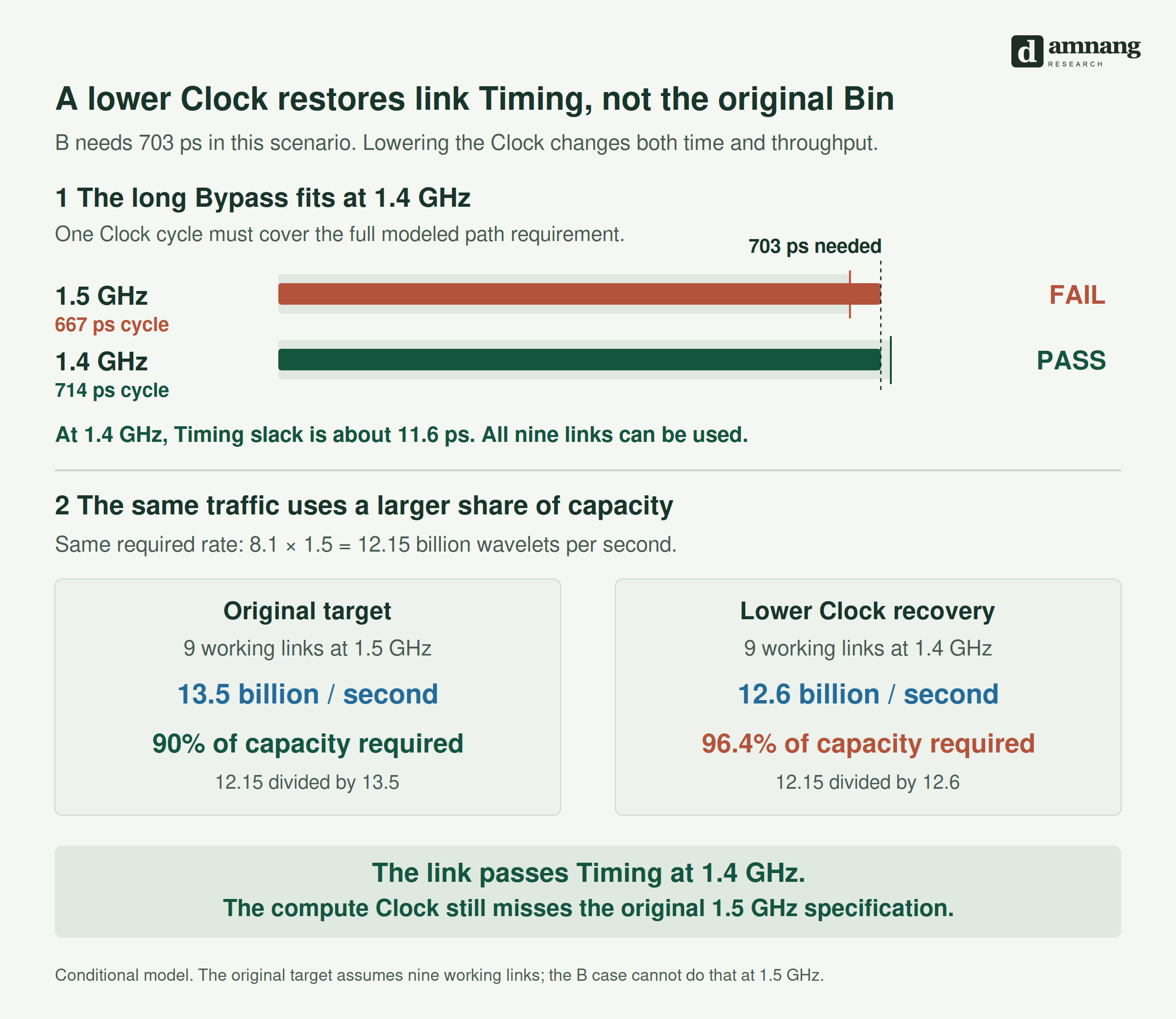
Applying a public wiring model and assumed circuit delays to the dedicated bypass, both A and B pass at 875 MHz. Both still pass under the baseline conditions when the target frequency is raised to 1.5 GHz. Under the worsened delay conditions, however, B’s minimum required clock period rises to 703 ps, exceeding the 667 ps limit. Of the two configurations that secured 45 good PEs, B succeeds in repairing the connections but still fails to meet the target frequency specification.[11]
4. Parametric Failures Can Further Worsen Cerebras’s Yield
As seen in Section 3, using a long bypass to route around cluster defects increases wire delay. If delay changes caused by process, voltage, and temperature (PVT) are added to this, the target clock specification may not be met. Then how does yield change if this performance variation differs by location within the wafer?
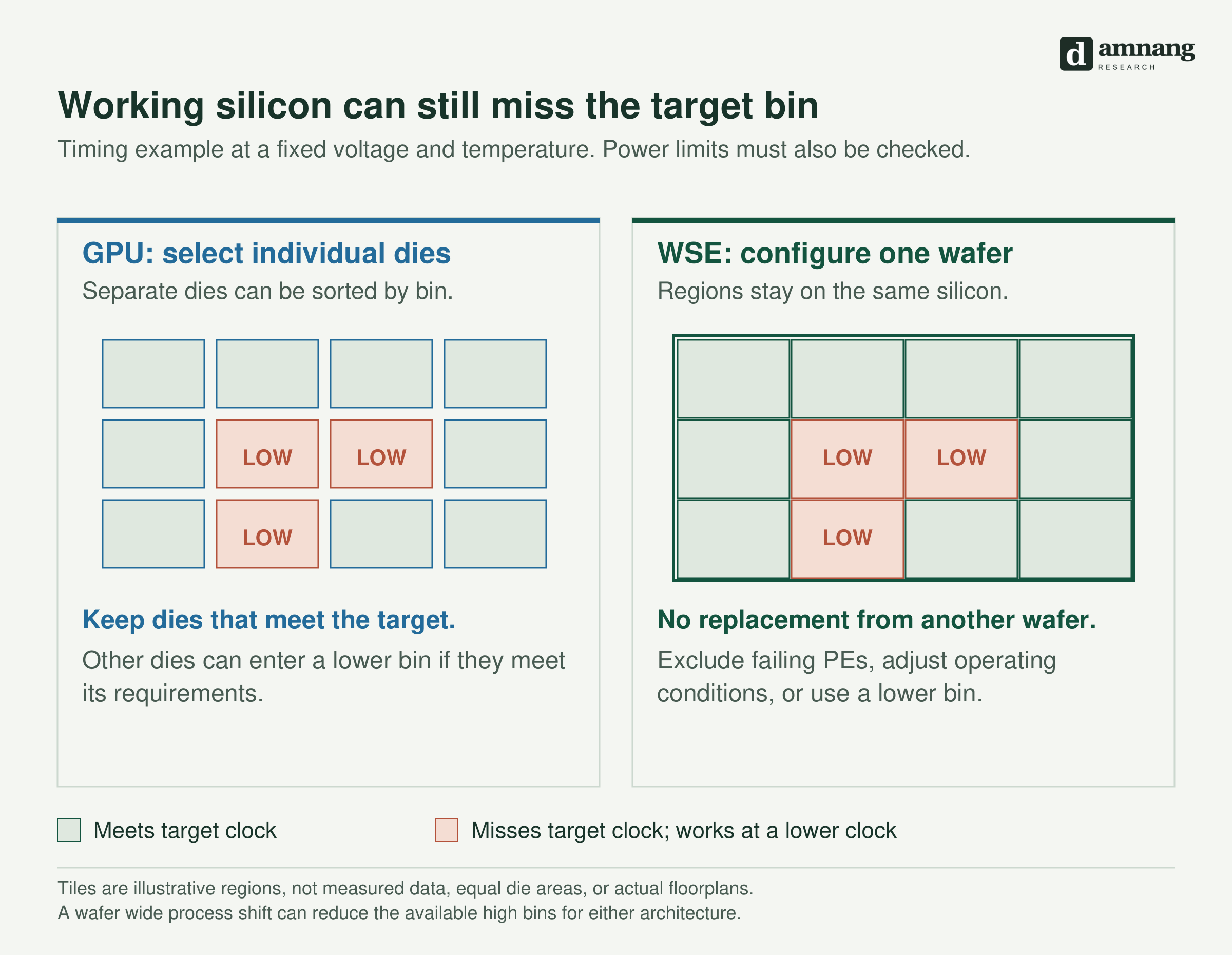
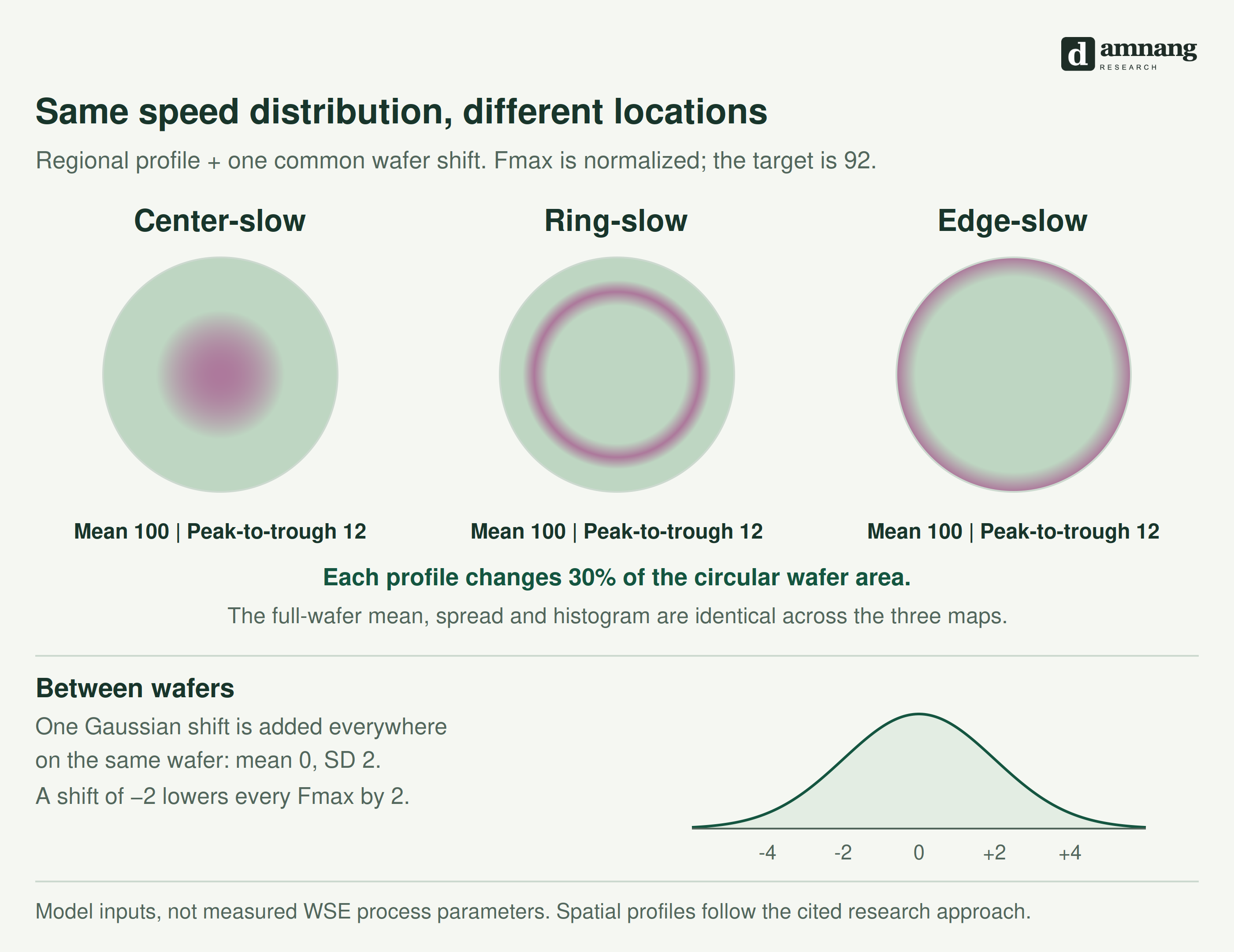
This time, I excluded the connection issues discussed earlier and analyzed only the effect of parametric failures related to PVT. Referring to spatial variation approaches in published research, I created three maps with slow regions at the center, in a ring, and at the edge. I kept the performance values and their area fractions identical across the circular wafer and changed only their locations.[15] [16] [17] With voltage and temperature fixed, I expressed maximum operating frequency, Fmax, as a relative value with a mean of 100 and set the target to 92. I checked whether the required number of TPCs meeting the target frequency remained on each GPU die, and whether the required number of PEs remained on a single WSE wafer.
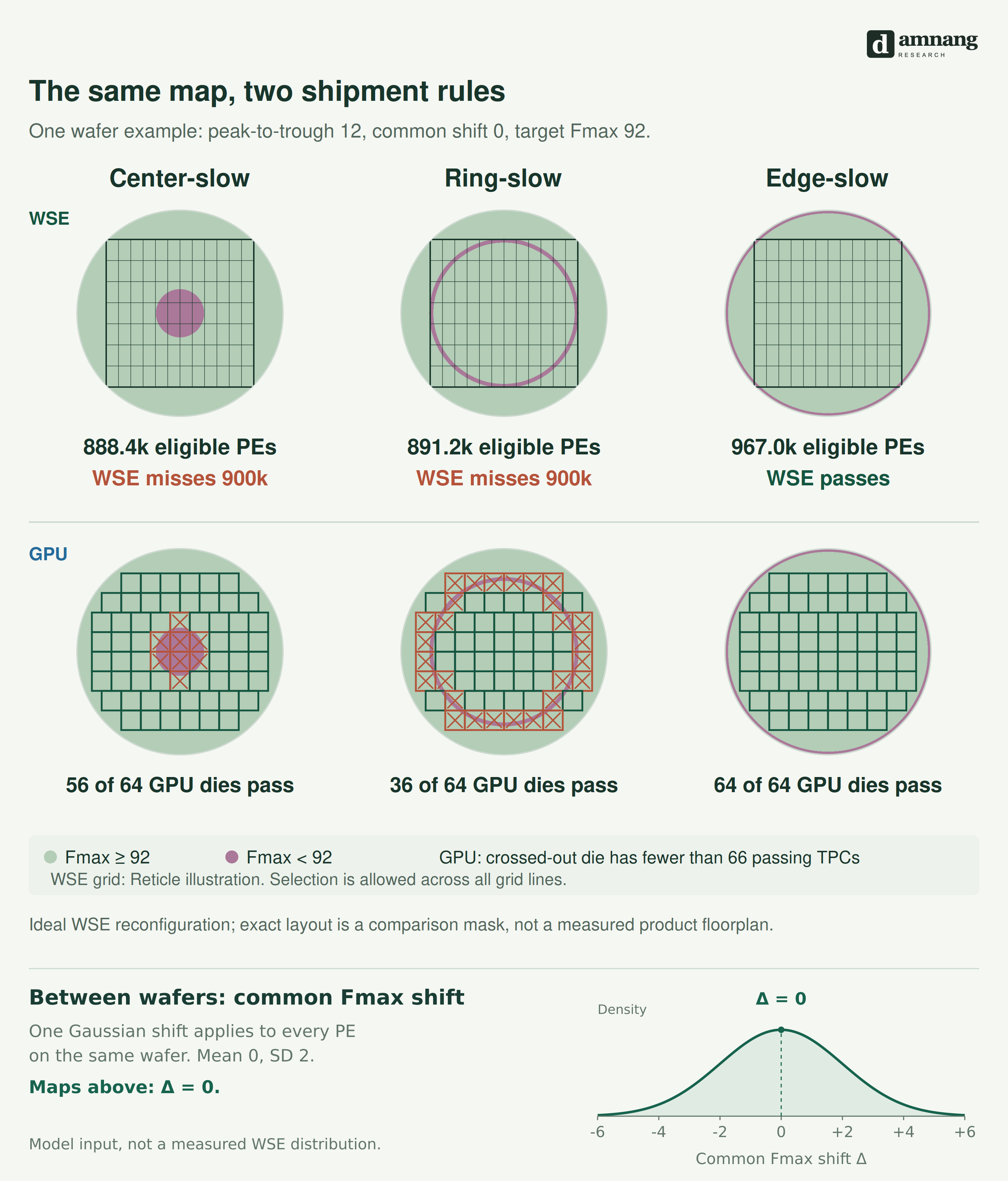
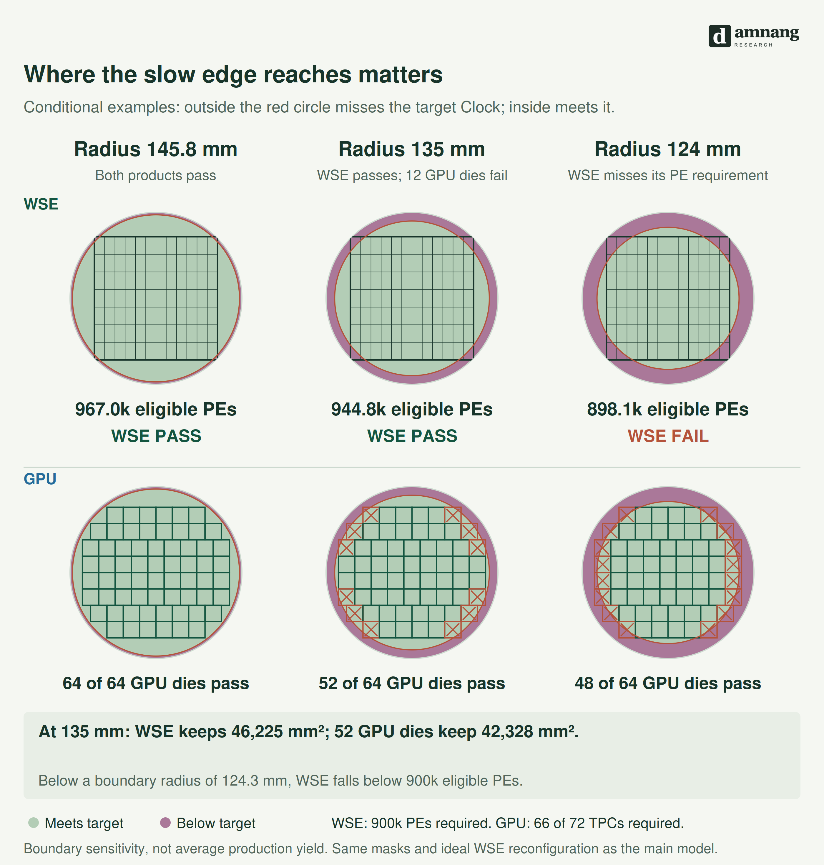
The difference in the two structures’ results comes from the unit at which regions below the performance requirement are excluded. If Fmax is low at the center, GPUs can exclude dies that fail the specification and ship the other dies. WSE must secure 900,000 PEs on the same wafer, so if spare PEs cannot replace a wide region below the performance requirement, that entire wafer falls short of the specification.
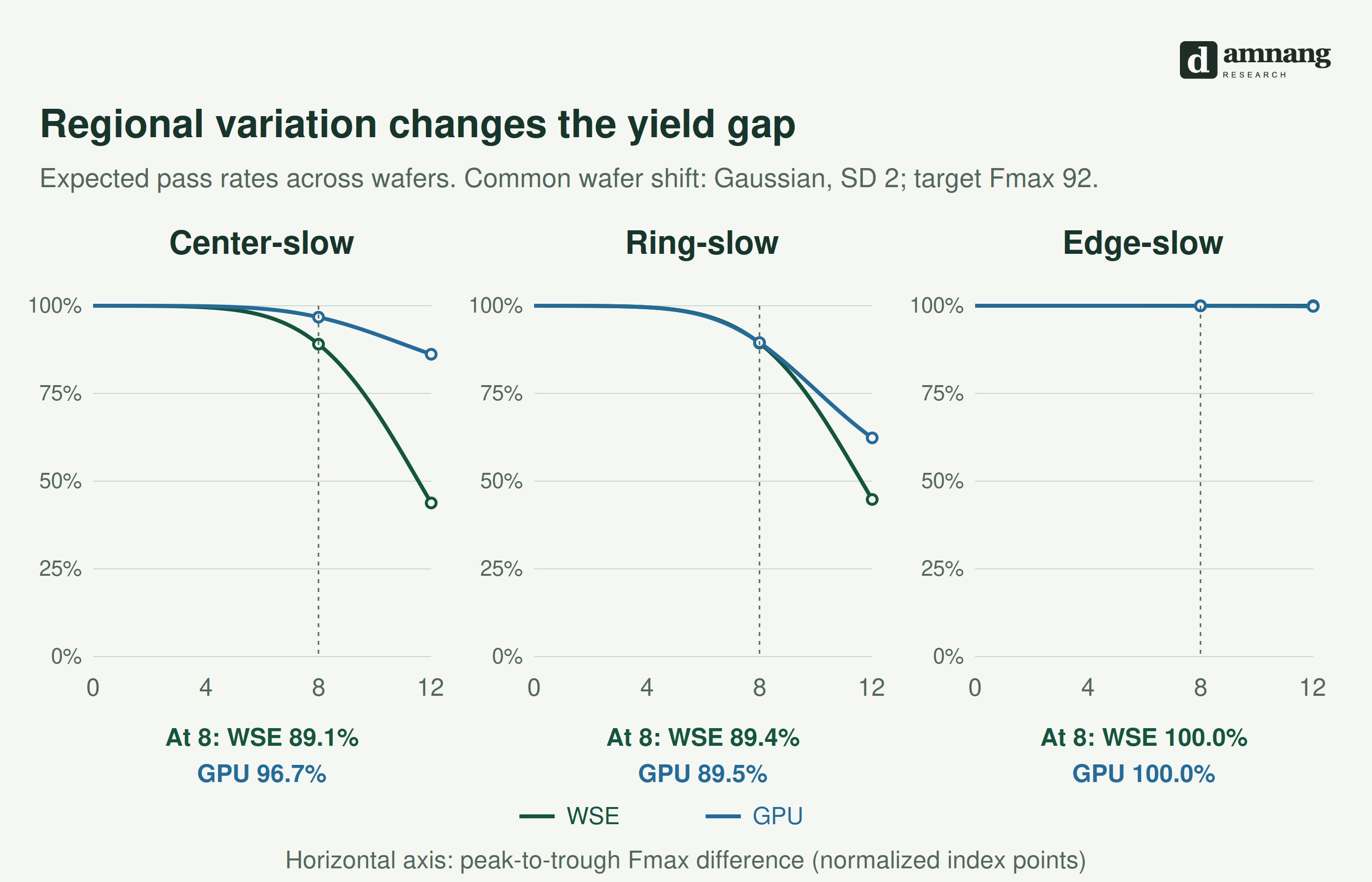
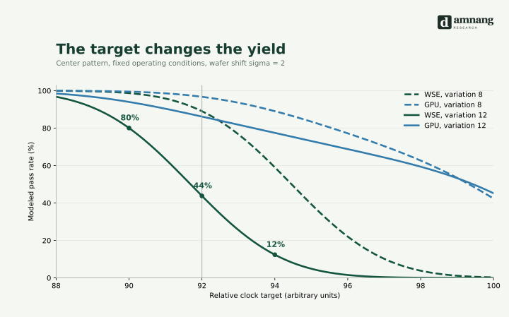
The figure shows the result for one wafer. Even with the same spatial distribution, the overall Fmax level can differ from wafer to wafer. When I applied this variation across multiple wafers, the WSE wafer pass rate was about 44%, while the average GPU die pass rate was about 86% in the scenario with a large center variation.
In this model without connection constraints, the value that determines whether WSE passes is not the average Fmax, but the Fmax of the 900,000th fastest PE. Even if average performance is high, the required PE count cannot be secured if this value is below the target. As the curves below show, raising the target frequency reduces the number of passing PEs and lowers the wafer pass rate.
For reference, these results are not always unfavorable to WSE. If the performance degradation is at the edge, it may overlap less with WSE’s actual footprint and favor WSE. If it forms a ring, it can affect many GPU dies and reduce the benefit of screening individual dies. Yield therefore depends not only on average performance, but also on the extent to which the region below the performance requirement overlaps the product area.
5. Wafer Scale Chips Can Incur Higher Test Costs
Even High TR Coverage Can Miss a Slow Path
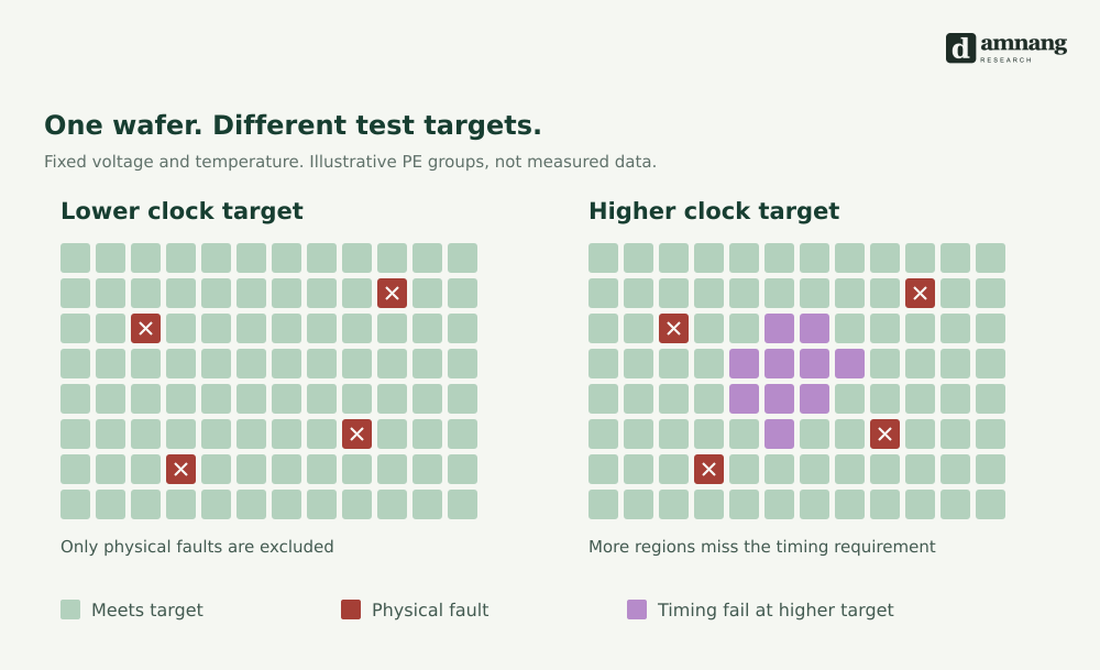
The transition delay fault model (TR) is a common fault model for at speed testing that examines timing margin. It is suitable for checking slow to fall and slow to rise faults at a specific node, but has limitations in checking the delay of a specific path. In this subsection, I directly implemented and measured a small PE circuit to examine these limitations of the TR model.
The example PE used in the experiment below consists of an 8 bit ADD/XOR unit and a router that selects one of the north, south, east, and west inputs. I injected stuck at faults (SA), which fix a node at a logic value, and transition delay faults (TR), and selected patterns through fault simulation that compares responses. As a result, eight SA patterns and 14 TR pattern pairs detected all 382 node faults in each model.
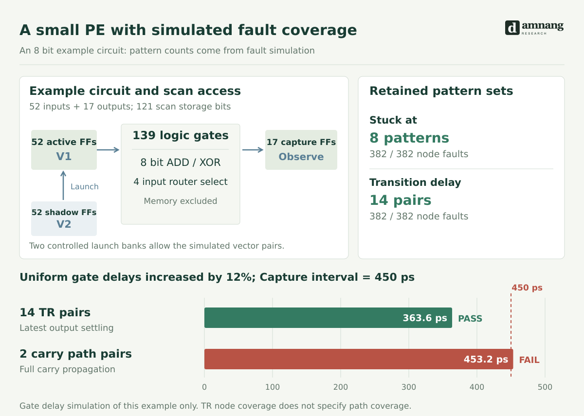
However, the result changed when I increased the gate delays in the same circuit by 12%. At a 450 ps interval, all existing TR patterns passed, but two patterns that activated the full carry path required 453.2 ps and failed. The patterns that detected node transition faults had not necessarily activated the slowest path.
Processing the Defect Map and Repair Settings for the Entire Wafer Takes Time
To calculate the repair and test burden across the entire wafer, I expanded the experiment to a 1,024×1,024 PE array, a scale similar to WSE-3’s approximately 970,000 PEs. Referring to the flow in Cerebras’s patent for recording defective PE coordinates, selecting a usable array, configuring repairs, and retesting, I built a mesh model that changes connections according to defect locations.[1][2]
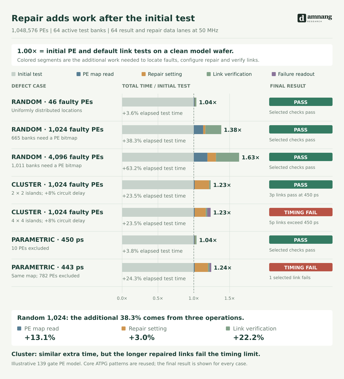
I grouped 32×32 PEs into one test region, creating 1,024 regions in total, and broadcast the same patterns to up to 64 regions. Responses are compared and stored for each PE, and detailed results are read from failed regions to determine repair locations.[18] I used 64 serial channels at 50 MHz for result readout and repair configuration. I set the initial PE and default connection test time for a defect free wafer to 1, then calculated the additional time for defect readout, repair configuration, and testing modified connections. Differences caused by channel count are compared separately in the appendix.
For random defects, the test time required for repair increased as defects spread across more regions. With 46 defects, testing took about 4% longer than the initial test. When I increased the defect count to 1,024, detailed results had to be read from 665 regions and 2,041 repaired connections had to be tested. Defect readout added about 13% of the initial test time, repair configuration about 3%, and connection testing about 22%, increasing total time by about 38%. With 4,096 defects, the increase was about 63%. The common PE test patterns remained the same, but the amount of additional work changed with the defect map.
For cluster defects, repair outcomes differed even with similar additional test times. I arranged 1,024 defects in 2×2 or 4×4 groups and applied the same 8% increase in circuit delay to both. Both cases took about 23% longer than the initial test. However, the 3p connections bypassing the 2×2 groups passed the 450 ps specification, while the 5p connections required for the 4×4 groups failed at 460.4 ps. In the latter case, the configuration could not be used even after repair configuration and connection testing were completed.
For parametric failures, shortening the target period increased both the number of PEs to exclude and the amount of repair testing. On the same speed map, setting the target to 450 ps produced a passing configuration with 10 PEs excluded, taking about 4% longer than the initial test. At 443 ps, the number of PEs to exclude rose to 782. Total test time increased by about 24%, after which one repaired connection failed the timing test. Even after screening PEs that failed the speed requirement, an additional test was needed to determine whether the configuration connecting the remaining PEs met the target period.
In this model, even repairable defects required additional test time. This was because, after defects were found in the initial test, repair configuration and verification of the selected paths still had to be performed. With the same equipment and hourly rate, this additional time increases the cost of that test process. The test cost of a structure that repairs an entire wafer at PE granularity must therefore include not only initial defect detection, but also the cost of configuring and verifying each wafer’s repair configuration.
The fact that the selected repair configuration can fail even after additional testing can further increase test cost per good unit. If a wafer is rejected for a timing failure after repair, as in the cluster and parametric cases, the test time spent on that wafer is reflected in the cost per good unit along with the test time spent on passing wafers. This is why the number of good units recovered through repair must be considered together with the test time the repair process requires.
6. These Problems Can Worsen with Turbo
Cerebras says it doubled Turbo’s compute performance and SRAM and fabric bandwidth by improving the power delivery and cooling structures of the same WSE-3 silicon.[19] [14] It places power converters close to the wafer to reduce resistive losses along the path supplying large currents, delivering about twice the power at nearly the same voltage.[23]
But as with all semiconductor design, there is no free lunch. A higher target frequency means less delay is allowed in PE internal circuits and repair connections. Even if improvements in power delivery and cooling reduce actual delay, PEs or long bypasses with insufficient delay reduction may fall short of the new specification. Also, excluding more PEs that fail the speed requirement can make repair paths longer, and a shorter timing limit may apply to those paths. This means the additional test costs analyzed in Section 5 could become more severe.
A Long Bypass That Previously Passed May Fail the Higher Speed Specification
The cluster defect case in Section 3 failed timing because of the long bypass, even after good PEs had been connected. This means a connection that was acceptable at a lower frequency may exceed the specification when the target period is shortened. With Turbo, the timing of an existing repair configuration can become a problem even without additional defective PEs.
Improving power delivery does not change the length of signal wires fabricated on the same silicon. We cannot assume that wire RC delay and mux delay improve at the same rate as the internal PE circuitry. Under a higher speed specification, even a wafer with enough spare PEs may therefore be rejected because of long repair connections. This is a case where the connection conditions seen in Section 3 limit the configurations that can pass for a higher speed product.
More PEs Failing the Speed Requirement Can Also Make Repair Connections Longer
When the spatial variation from Section 4 is added, the repair configuration itself changes. If raising the target frequency excludes several PEs together in a slow region, it can both reduce the number of usable PEs and increase the distance needed to bypass that region. Even if average performance improves, there are two possible reasons for failure: not securing enough PEs, or the connections between the secured PEs failing the higher speed specification.
This second problem becomes visible if we keep the delay map from Section 5 unchanged and shorten only the test interval. At 444 ps, a connection skipping three PEs passed at 372.4 ps. At 443 ps, one more PE failed the speed requirement, so four PEs had to be skipped. The new connection’s delay increased to 459.3 ps and it failed. The allowed time decreased by 1 ps, but the delay increased by about 87 ps as the selected connection changed.
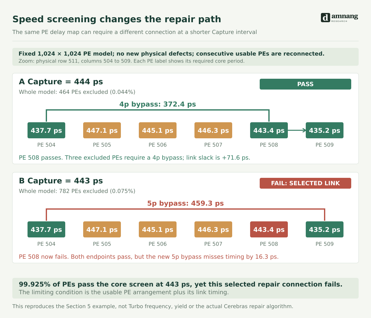
Even at 443 ps, 99.925% of all PEs passed the speed test. There was headroom in PE count alone, yet the selected repair configuration failed. This example does not calculate Turbo’s actual frequency or yield. It shows that the PE arrangement left by speed screening can sharply increase connection delay. Yield at a higher speed specification is affected both by how many slow PEs are excluded and by which connections are then required.
A Wafer Can Fail the Higher Speed Specification Even After More Test Time Is Spent
The same changes also create an additional testing burden. The high fault coverage of conventional transition delay patterns seen in Section 5 does not by itself guarantee the delay of the long paths actually selected. To avoid missing repair paths with reduced margin at the higher speed specification, patterns must observe transitions along the long paths under the corresponding mux selection settings. If existing patterns do not adequately test these paths, they must be supplemented with transition or path delay patterns that incorporate timing information.[21]
Even when patterns can be reused, repair configuration and result readout take time. In the same model, shortening the test interval from 450 ps to 443 ps increased the excluded PE count from 10 to 782, and the time to write repair settings from 10.2 μs to 321.3 μs. In this case, SA and TR patterns were neither regenerated nor reapplied. Parallel testing kept defective PE readout and connection test times almost unchanged, but the time to write repair settings sequentially increased because those settings were concentrated in a particular test region.
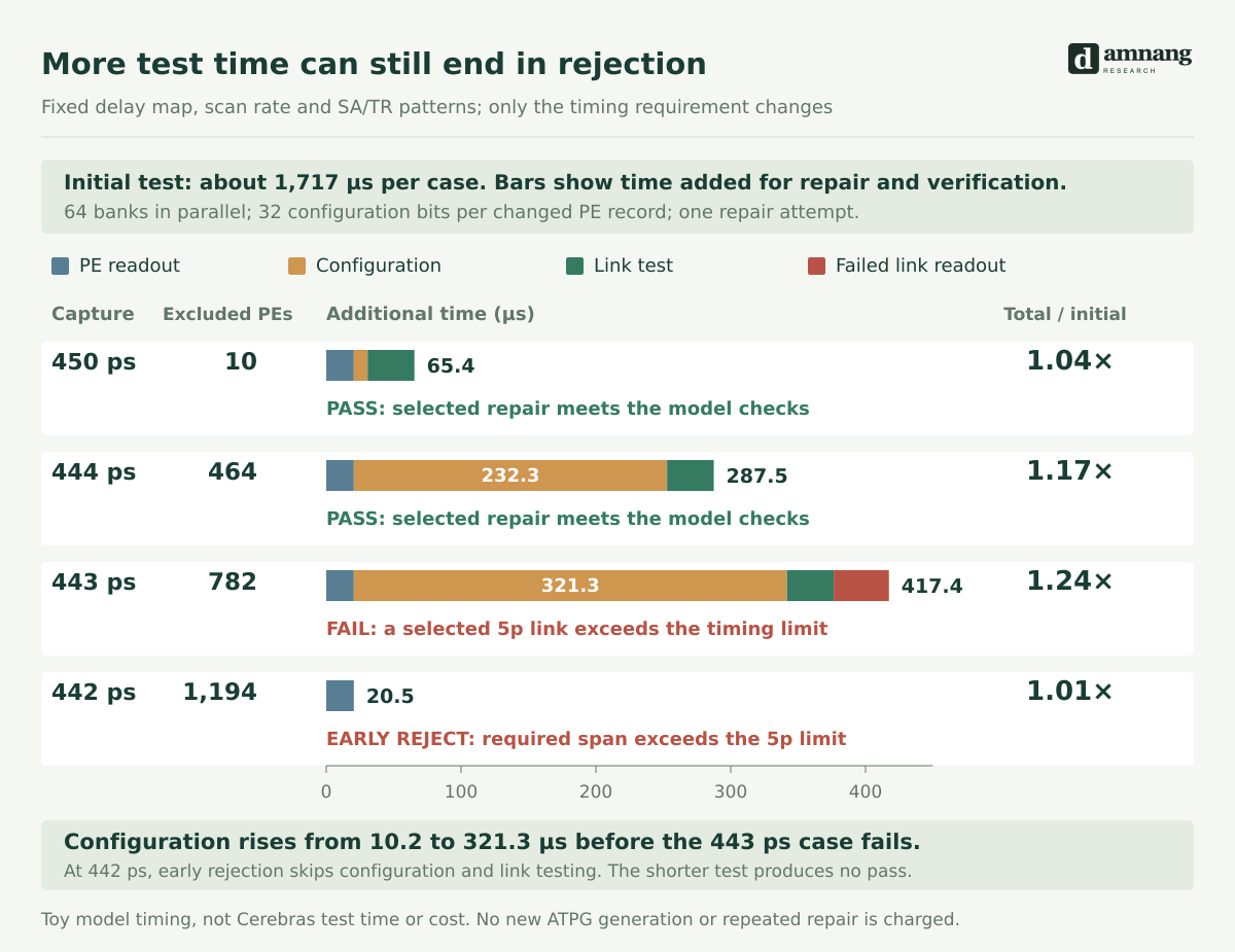
Total test time increased from 1.04 times to 1.24 times the initial test time, but the 443 ps configuration ultimately failed connection timing. At 442 ps, the time becomes shorter again because the selected repair rule’s connection span limit is exceeded and the process stops early. This is not an improvement in test efficiency. It is the result of being unable to proceed with repair configuration and subsequent testing. If repair attempts continue by searching for another configuration, more time is needed to retest the changed settings and paths. That repetition is not included in this calculation.
The point where Turbo’s mass production burden can increase is that fewer repair configurations may pass the higher speed specification, while the test time spent before determining a failure may increase. If timing failures reduce the number of wafers that can be shipped, there are fewer good wafers from which to recover manufacturing costs. The cost of wafers rejected after repair and testing is also reflected in manufacturing cost per good wafer. Raising operating frequency through better power delivery and securing enough repairable wafers at that frequency are separate mass production challenges.
Conclusion - We Need to Look at Yield and Test Costs After Repair
In the models in this article, what changed whether WSE passed was not just the number of defects, but their locations, PE speeds, and repair connection delays. When the target frequency rises, as with Turbo, fewer repair configurations may pass, while the test time spent before determining a failure may increase.
Cerebras’s competitiveness in mass production should therefore be evaluated by the proportion of wafers that meet the target specification after repair and the repair and test cost per good wafer. The spare PE count and the 164 times area comparison alone cannot explain these two conditions.
References
Public Specifications, Patents, and Papers
Cerebras, 100x Defect Tolerance: How Cerebras Solved the Yield Problem · January 13, 2025. The company’s comparison assumptions include a PE area of about 0.05 mm², spare cores, a defect density of 0.1 defects/cm², and a layout of 72 GPUs. Page 4 of a separate WSE-3 white paper gives a core area of about 0.038 mm², so I did not treat 0.05 mm² as an exact measured floorplan value. The blog explains both the advantages of small cores and cases where clusters exceed repair limits.
Cerebras, US11328208B2: Processor element redundancy for accelerated deep learning · I referred to the testing, defect map, array configuration, optional retesting, and frequency, voltage, and current qualification in FIG. 33; repair connections and equal cycle latency in FIG. 34 and 35; and selective exclusion of good resources, counts per column, adjacent connection constraints, and balancing of power distribution in FIG. 38B. These are patent embodiments, not confirmed actual production algorithms or test coverage for WSE-3/Turbo.
Sean Lie, The Cerebras Wafer-Scale Architecture for Deep Learning, WSE-3 white paper · Pages 3 and 7 of the official white paper explicitly identifying WSE-3 as the subject. I confirmed the 84 die configuration in the text. The illustration on page 7 is labeled WSE-2, so I used its 12 columns and 7 rows only as a reference for conceptual diagrams and hypothetical grids. PE allocation per region and repair limits are separate analytical assumptions. I also referred to SRAM per PE, the router with five ports, communication with neighbors in one cycle, colors, lossless flow control, and compensation across reticle boundaries on pages 3, 7, and 8.
NVIDIA, NVIDIA Hopper Architecture In-Depth · March 22, 2022. I confirmed GH100’s area of 814 mm² and 144 SMs, H100 SXM’s 132 active SMs and 66 TPCs, and the TSMC 4N process. Pass rates under defects at SM/TPC granularity are calculated using this article’s hypothetical models.
NVIDIA, Virtualizing Hardware Processing Resources in a Processor, US20260023112A1 · Describes floorsweeping that disables defective circuitry through fuses or other means, screening by the number of good TPCs, and reassignment of logical indices. It is not treated as a disclosure of H100’s specific production test rules.
TSMC, 5nm D0 Trend, 2020 Technology Symposium presentation slide · An archived image of presentation material from August 2020. I read approximately 0.3 to 0.33 three quarters before N5 mass production and approximately 0.1 to 0.11 around the start of mass production from the curve. The dotted line is the forecast at that time. The forum poster’s interpretation was not used as data.
Intel, Q3 2024 earnings call Q&A · Pat Gelsinger’s answer to Timothy Arcuri’s question. Management directly explained that an 18A D0 below 0.4 was good at that development stage, but not yet at HVM yield levels and needed to fall further. Full transcript archived by TickerTrends.
TSMC, official 2020 Technology Symposium announcement · August 25, 2020. Official announcement confirming the start of N5 volume production in 2020 and improvements in defect density. It does not disclose current measured N5 D0.
Cerebras SDK, Wafer-Scale Engine Architecture · Fabric router and compute engine in each PE, connections to four neighbors, the 2D mesh, and transfer of a 32 bit wavelet in one cycle. Actual router delays at gate level are not disclosed.
Belli·De Sensi, Stencil Computations on Cerebras Wafer-Scale Engine · May 8, 2026. I used the 875 MHz nominal frequency in the WSE-3 experimental methodology as the baseline operating point. It is not interpreted as the guaranteed or maximum clock of all WSE-3 products.
OpenROAD, Correlating RC Values for PDKs · I used examples of RC per unit length extracted from ASAP7 designs and the stated units of kΩ/μm and pF/μm. M4, M6, and M8 values were adopted as comparison inputs, not substitutes for TSMC N5 characteristics.
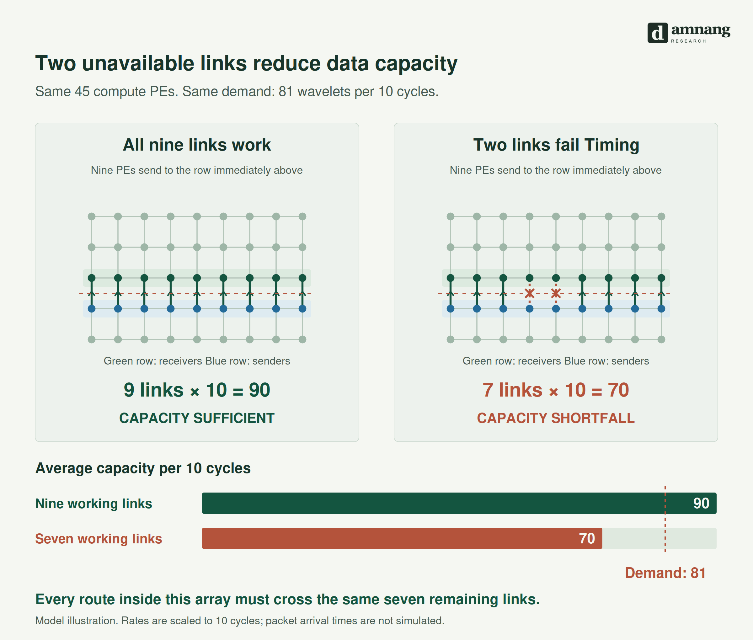
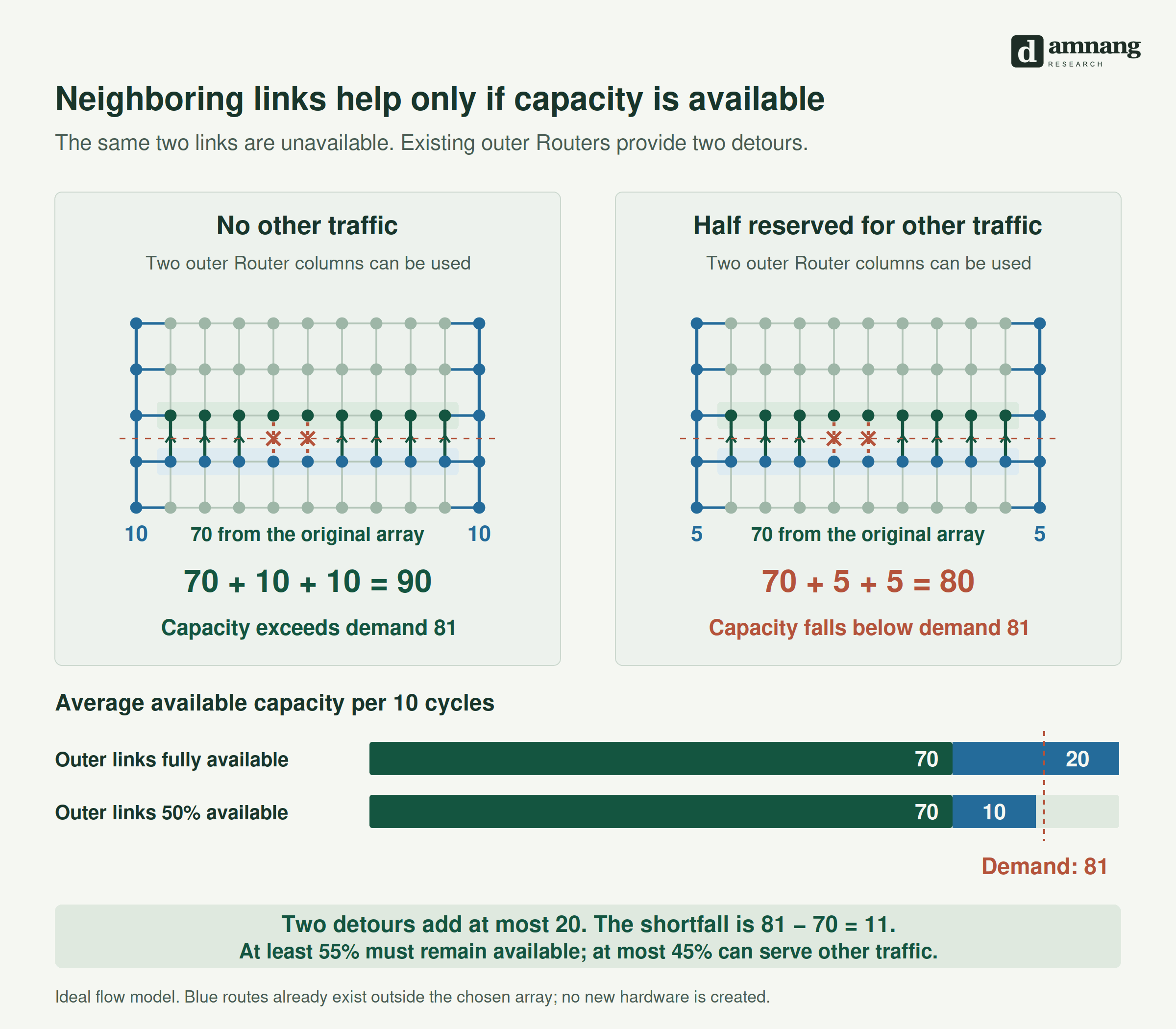
Cerebras SDK GUI, Timeline: Wavelet Traces · Distinguishes the Delayed state, where multiple inputs contend for an output router, from Backpressure, where the receiver cannot accept data. This supports distinguishing physical timing of a link that operates in one cycle from actual waiting time for delivery. Cut bandwidth and rerouting results in the appendix are my own calculations.
Cerebras SDK, Data Structure Descriptors · CE transmit and receive queues, microthread resources, and restrictions on simultaneous use. This supports the point that actual execution requires resource allocation in addition to path capacity. Queue depth was not used as router internal buffer depth.
Cerebras, Ultrafast Frontier Inference: Cerebras Deep Dive at Hot Chips 2026 · August 25, 2026. Improvements in power delivery and cooling, approximately twice the power at nearly the same voltage, and the structure and replacement method for individual wafer modules. I did not infer shipment pass rates by frequency or speed screening policies from this presentation.
Yin·Chen·He·Li, Data Efficient Prediction of Minimum Operating Voltage via Inter- and Intra-Wafer Variation Alignment · VTS 2025, DOI 10.1109/VTS65138.2025.11022948. The preprint was released in August 2024. It analyzes Vmin of actual 16 nm automotive chips and separates variation between wafers and between regions. The main text uses a separate Fmax scenario informed by that decomposition approach.
Yin·Chen·Xu·He·Li, Transfer Learning for Minimum Operating Voltage Prediction in Advanced Technology Nodes: Leveraging Legacy Data and Silicon Odometer Sensing · ITC 2025. Covers 415 chips at 5 nm, 124 silicon odometer inputs, and DC scan, AC scan, and MBIST Vmin. Cited as evidence of using spatial and circuit specific information in actual 5 nm devices. The measurements were not used as the mean or standard deviation of WSE Fmax.
Sarkar·Lowe·Vincent, Virtual Semiconductor Fabrication: Impact of Within-Wafer Variations on Yield and Performance · 2025 Winter Simulation Conference, a two page research summary. A Lam Research model of virtual 14 nm FinFET manufacturing and process variation. I referred to its comparison of center, edge, and donut spatial patterns. The functions in the main text that move locations while retaining the same distribution, and the Fmax amplitude, were defined separately by the author.
Siemens, No-compromise packetized test improves DFT efforts · January 30, 2025. Describes broadcasting patterns, expected values, and masks to repeated cores, comparison and result storage within each core, and independent shift and capture control. This is not a claim that Cerebras uses this solution.
Cerebras, Cerebras Unveils CS-4: Up to 30 Times Faster than GPU-based Solutions · Announced August 18, 2026. Specifies doubled compute performance and SRAM and fabric bandwidth for WSE-3 Turbo, and increased operating frequency from improved power delivery. It does not provide exact internal clock values or shipment yields by frequency.
Kleveland·Ferolito·Morrison·Scherer, Wafer-Scale Integration for AI: The Holy Grail? · Cerebras, 2025 Symposium on VLSI Technology and Circuits, JFS3-1. The abstract on printed page 50 of the official Advance Program specifies adoption of in system burn in and HTOL using heated coolant. This is not used to imply that the same HTOL test is applied to every shipped unit.
Synopsys, TestMAX ATPG · Distinguishes fault models including conventional transition, slack based transition, path delay, and hold time, as well as integration with STA and wire extraction tools. This supports general DFT capabilities, not Cerebras’s adoption of a particular tool.
Ron Press, Test Points are Trending · Siemens/Mentor Graphics, October 14, 2015. Describes the transition fault model targeting large delays, timing aware ATPG that considers actual paths, path shortening through observe test points, and path delay patterns.
Jean-Philippe Fricker, explanation of design changes after the CS-4 launch · Public explanation by Cerebras’s cofounder. Distinguishes the 54.5 V DC path, DC/DC conversion in the backpack, an approximately 0.5 mm power delivery path, about twice the current at nearly the same voltage, and improvements in component count and assembly structure. The 100 times comparison in delivery distance is against a conventional GPU board. Improvements in manufacturing cost and first pass yield are qualitative company claims without yield figures.
Appendix
This appendix collects structural explanations and calculations left out of the main text. The numbers below are also model results, not actual product measurements.