

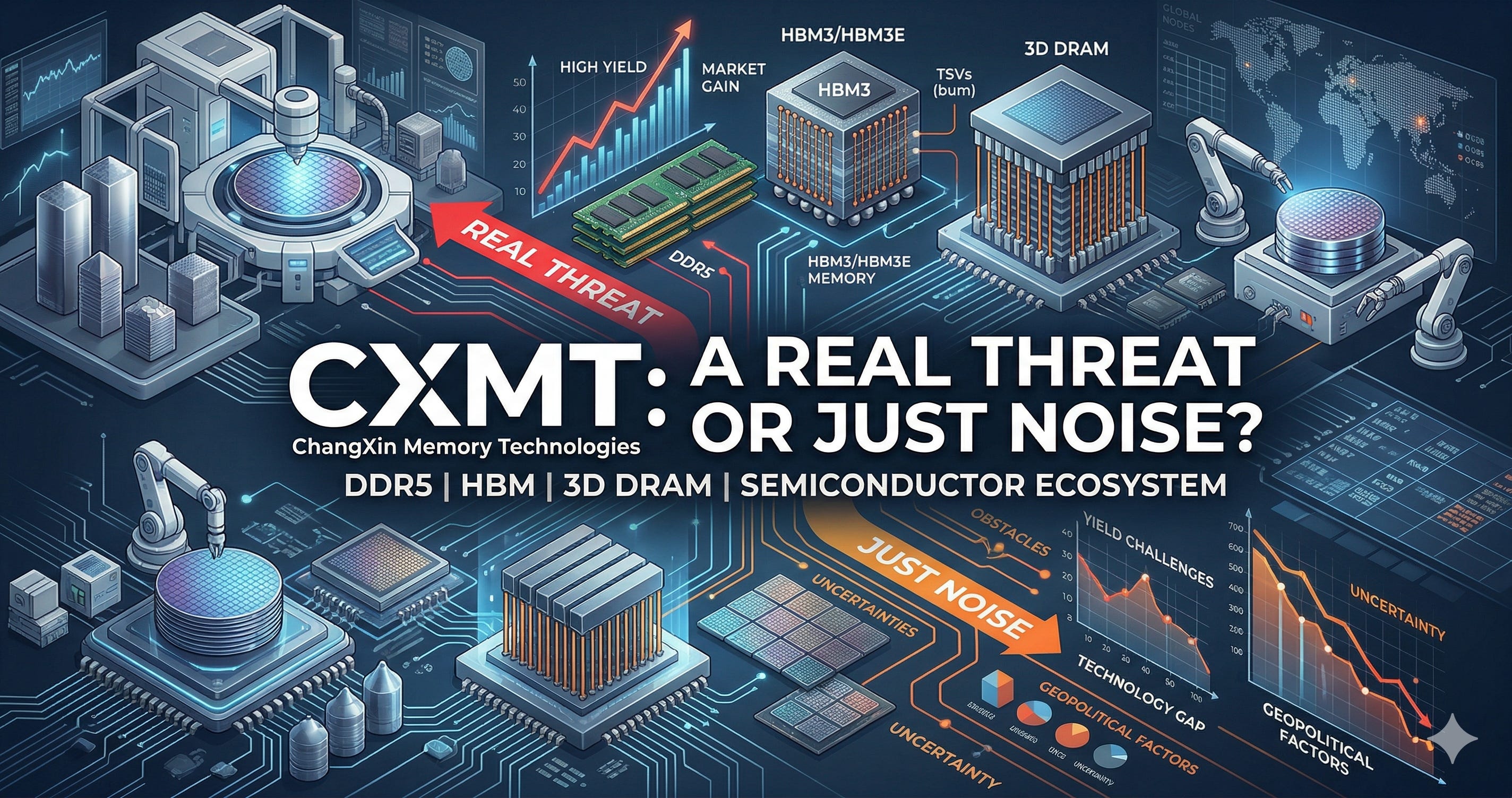
CXMT (长鑫存储, ChangXin Memory Technologies) is China’s largest DRAM company. Revenue surged in 2025, and the company is now pursuing a Shanghai IPO with a target valuation reportedly in the $42 billion range. It is already considered the world’s fourth-largest DRAM player by capacity.
The market still tends to view CXMT as just “China’s late-arriving DRAM maker.” But look at the products one by one, and the story changes. DDR5 is already shipping inside Lenovo laptops. LPDDR5X accounts for roughly 30% of the Chinese smartphone market. HBM still has a wide generational gap, but within the context of China’s domestic AI supply chain, it is not something you can dismiss simply as “behind.”
The point that deserves the most attention is 3D DRAM. In 3D DRAM, there is a real possibility that the entire competitive landscape gets redrawn.
I recently had the chance to speak separately with the head of SK hynix’s Americas operation and a current ASML employee. Both had weighty things to say about China’s 3D DRAM efforts. I will get into the details later, but after those conversations, I came away with a strong sense that China’s 3D DRAM capabilities should not be taken lightly.
In this article, I will first lay out where CXMT stands today, then break down how far it has actually gotten in DDR5 and LPDDR5X sales, why HBM still has a significant gap, and how 3D DRAM and the equipment ecosystem factor in to what kind of variable this company could become for the memory industry.
Table of Contents
Where CXMT Stands Today
Commodity DRAM: The Opening Is Already There
HBM, Where the Biggest Gap Remains
3D DRAM, Where the Game Gets Flipped
What 3D DRAM Changes: Not Just CXMT, but the Entire Equipment Ecosystem
What Actually Changes for the Big 3
Threat or Illusion
This article does not constitute a recommendation to buy or sell any specific security. All investment decisions are solely the responsibility of the investor.
Where CXMT Stands Today
CXMT’s starting point was 2016. Backed by China’s Big Fund semiconductor self-sufficiency initiative, the company built a 12-inch DRAM fab and began volume production with 19nm DDR4 and LPDDR4. Wafer output, which stood at around 40,000 wafers per month in 2020, has reportedly grown to approximately 720,000 wafers per quarter by the end of 2025. The company now operates three 12-inch DRAM fabs.
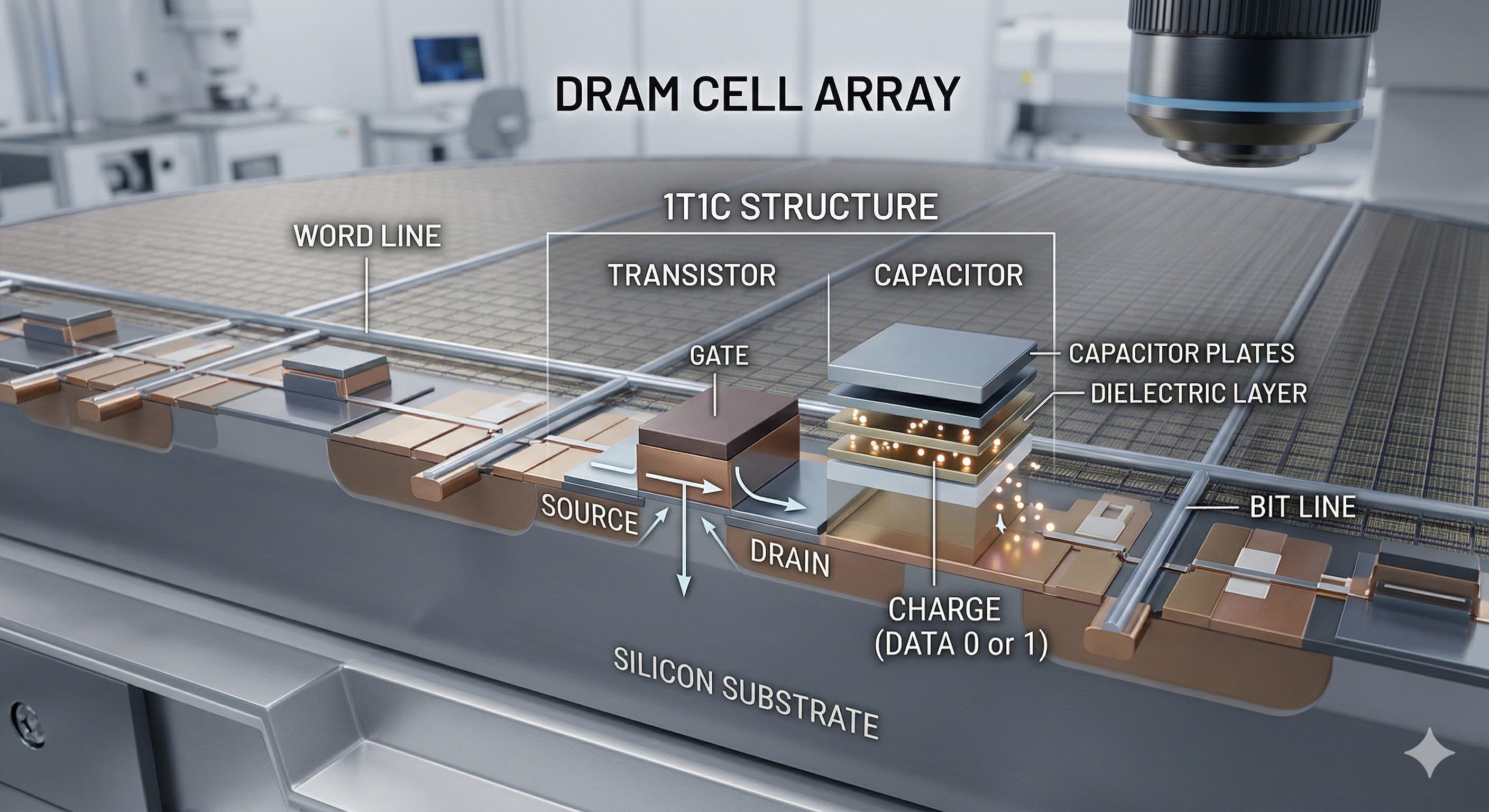
To understand why that number matters, it helps to cover the basics of DRAM process technology. DRAM is a memory semiconductor that stores data, and each memory cell consists of one transistor and one capacitor in what is known as a 1T1C structure. The transistor acts as a switch for reading and writing data, while the capacitor stores charge to represent 0s and 1s. Ultimately, DRAM competitiveness comes down to how small and precisely you can make that cell.
Process shrinking means reducing the size of this cell. Smaller cells mean more cells fit into the same area, chip capacity goes up, and more chips come off a single wafer. The result is lower cost per bit. This is why Samsung, SK hynix, and Micron are obsessed with the race through 10nm-class nodes like 1a, 1b, and 1c.
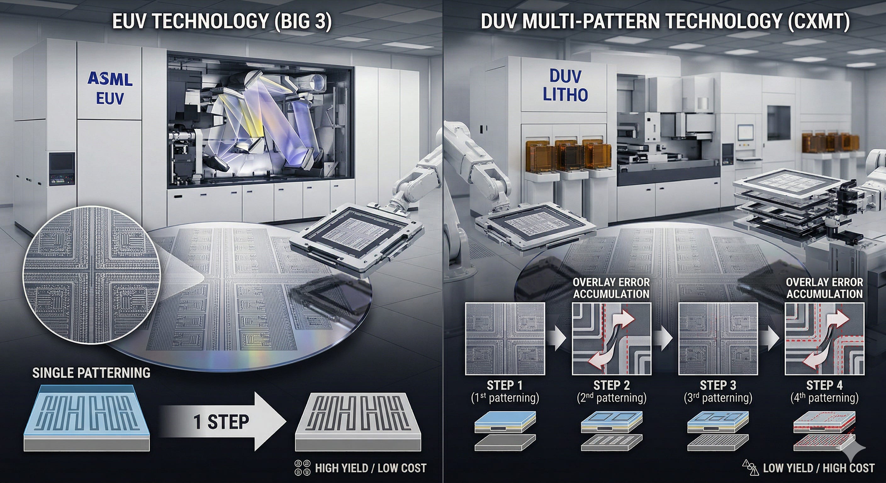
The challenge is how you implement that shrink. The Big 3 use ASML’s EUV lithography tools to achieve finer patterns with relatively fewer process steps. CXMT, however, cannot access EUV equipment due to US-led export controls. So it relies on DUV tools and multi-patterning to achieve the same level of patterning. Circuits that cannot be printed in a single exposure are split across two or even four passes. This adds process steps, and each additional step accumulates overlay errors, putting CXMT at a disadvantage in yield and cost.
Despite this, CXMT has pushed its way up to its G4 node using DUV multi-patterning alone. G4 is an internal generation label. According to TechInsights analysis, the G4 feature size is around 16nm, roughly a 20% cell size reduction from the previous G3. The Big 3 were already in volume production at the 16nm level around 2018 to 2019, which puts the gap at five to six years or more. The fact that CXMT got here without EUV is precisely why the industry started taking it more seriously. It is also the backdrop to Seoul National University Professor Hwang Cheol-seong’s assessment that CXMT could produce 11nm-class DRAM without EUV.
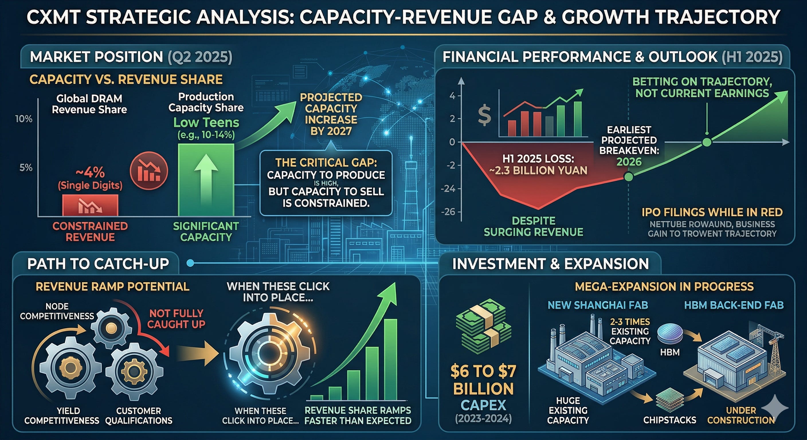
So where does the business stand? In terms of revenue-based global DRAM market share, CXMT was at roughly 4% as of Q2 2025, still in the single digits. But its share of production capacity has already climbed into the low teens and is expected to expand further by 2027. The capacity to run wafers is already significant, but the share of products it can actually sell remains limited. Node competitiveness, yield, and customer qualification have not fully caught up yet. Once those three align, the revenue share could climb faster than people expect.
The financials reflect this structure directly. According to Reuters, citing IPO filings, CXMT posted a loss of approximately 2.3 billion yuan in the first half of 2025 despite surging revenue. The earliest breakeven is projected for 2026. Pursuing an IPO while still in the red means the market is betting on future growth rather than current profits. CXMT reportedly invested $6 to $7 billion in capex between 2023 and 2024, and it is building a new DRAM fab in Shanghai that is two to three times the size of its existing fabs. A separate HBM back-end fab is also under construction.
CXMT is not yet a finished powerhouse. Its technology trails the Big 3, its revenue share is still low, and it is losing money. But production capacity has already reached the global top four, and once product competitiveness and customer qualification fall into place, the numbers can shift quickly.
Now let’s go product by product.
Commodity DRAM: The Opening Is Already There
Commodity DRAM is the general-purpose memory that goes into PCs, laptops, smartphones, and standard servers. DDR5, LPDDR5X, and server-grade RDIMM and MRDIMM all fall into this category. Unlike HBM, this market is not decided by a single overwhelming technology edge. What ultimately matters is whether you can build products at a certain quality level, whether you can actually supply customers, and how reliably you can push volume. By that measure, CXMT has already reached a position that is hard to ignore.
The key question is not whether CXMT has caught up with Samsung or SK hynix on technology. It has not. The more important point is that while the Big 3 pour resources into HBM, CXMT has started filling the vacancies opening up in the commodity space with real volume. The threat does not come from technology brochures. It comes from shipments and adoption.
LPDDR5X: Where It First Made Its Presence Felt
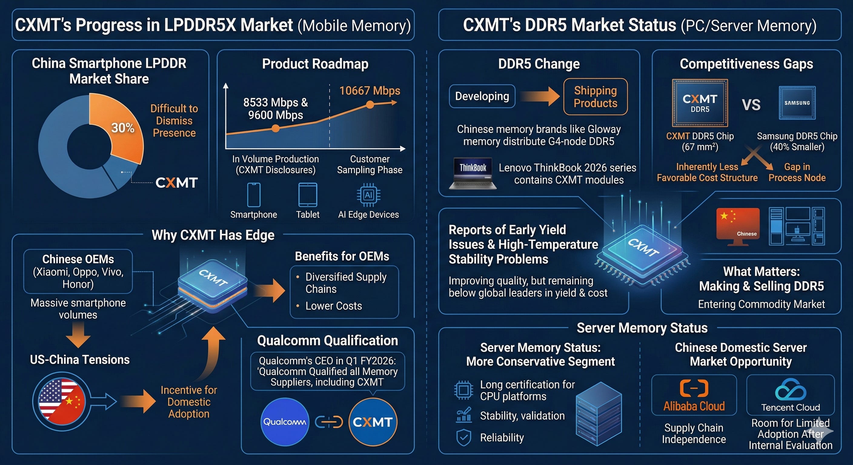
LPDDR5X is where CXMT first showed real muscle. LPDDR5X is a mobile memory used in smartphones, tablets, and AI edge devices, and in the Chinese domestic market, CXMT has already built a presence that is difficult to dismiss. According to CXMT’s own disclosures, its 8533 Mbps and 9600 Mbps products are in volume production, while the 10667 Mbps product is in the customer sampling phase. Per Caixin Global reporting, CXMT already holds roughly 30% of China’s smartphone LPDDR market. It would be premature to say that every speed grade is in stable mass production, but at least within the Chinese domestic market, the company is clearly generating meaningful volume.
The reason CXMT has an edge here is less about the technology itself and more about market structure. Chinese OEMs like Xiaomi, Oppo, Vivo, and Honor ship massive smartphone volumes every year. For them, CXMT memory is not just a domestic substitute. It is a practical option that diversifies supply chains while also lowering costs. The longer US-China tensions persist, the stronger the incentive to increase adoption of domestic components.
Qualcomm’s remarks add symbolic weight here. During the Q1 FY2026 earnings call in February 2026, CEO Cristiano Amon stated that Qualcomm is in a qualified state with all memory suppliers, including CXMT. That means the technical groundwork for Chinese OEMs to pair Qualcomm APs with CXMT memory is already in place. This does not yet signal large-scale global proliferation, but it is safe to say that in LPDDR5X, CXMT has moved past the market entry stage.
DDR5: Still Short, but Already Shipping
DDR5 is also seeing clear changes. DDR5 is the standard memory spec used widely in PCs and servers, and CXMT is no longer a company that only develops products in this space. G4-node DDR5 products are being distributed through Chinese memory brands like Gloway, and at Chinese semiconductor trade shows, CXMT has shown high-speed specs approaching the Big 3’s latest. In November 2025, Caixin Global reported that CXMT was supplying DDR5 to Lenovo, and by March 2026, reports emerged that some models in the Lenovo ThinkBook 2026 series had CXMT memory modules inside. This is not a candidate under review. It is a supplier whose parts are going into products that actually ship.
That said, you cannot call it on par with the Big 3 just yet. There are clear limits in manufacturing competitiveness. According to TechInsights, CXMT’s DDR5 chip die size is approximately 67 square millimeters, about 40% larger than Samsung’s equivalent product. Because of the gap in process node, even at the same capacity, fewer chips come off each wafer, and the cost structure is inherently less favorable. Reports of early yield issues and high-temperature stability problems reinforce these weaknesses. There are assessments that quality has improved enough to be usable for PCs, but it is still hard to say CXMT has achieved Samsung-level or SK hynix-level yield and cost competitiveness.
But in the commodity market, you do not need top-tier polish to be a threat. What matters here is that CXMT is now making DDR5, selling it, and getting it into customer systems. There is a bigger gap than people realize between a company that cannot build something and a company that ships it, even imperfectly.
Server memory is an even more conservative segment. CXMT has announced RDIMM and MRDIMM lineups, but servers are not like PCs where simply working is enough. You need CPU platform compatibility, long-duration stability, the customer’s own internal validation, and reliability testing in live data center environments. The certification process is longer and far more demanding. So the server side has not been cracked as quickly as the PC side.
That said, the Chinese domestic server market could be different. For local players like Alibaba Cloud and Tencent Cloud, the motivation goes beyond price. Supply chain independence matters. Even without following the same conservative validation frameworks that global hyperscalers use, there is room for limited adoption after internal evaluation. It may not be enough to shake the global server market right now, but the Chinese domestic market alone could become a meaningful source of demand.
The Real Story Is Structure, Not Products
What becomes even more important here is not the completeness of individual products but the structure of the industry. Samsung, SK hynix, and Micron are all concentrating wafer capacity on HBM right now. But HBM DRAM dies are significantly larger than commodity DDR5 dies. The same wafer yields fewer dies, and it takes far more capacity to supply the same amount of memory. The more the Big 3 lean into HBM, the tighter commodity DRAM supply gets in relative terms.
In this environment, the rules of the game change.
The winner is not the company with the perfect product. It is the company that has something ready to ship right now. When supply itself is tight, the value of an alternative supplier grows, even if quality is a step below the leaders. This is exactly where CXMT finds an opening.
There are already signs of this playing out.
In early 2026, Reuters re-cited Nikkei Asia reporting that HP and Dell had explored qualifying CXMT DRAM, and that Acer and Asus were also looking into the possibility of adopting Chinese-made memory. It is too early to say this has reached large-scale adoption. But the fact that global OEMs have stopped treating CXMT as a non-existent player and started viewing it as an alternative supplier they could use if needed is itself significant.
Putting It Together
The commodity DRAM threat from CXMT is not arising because its products are better than the Big 3’s. It is arising because while the Big 3 focus on HBM, CXMT has started filling the gap in the commodity space with actual volume. In LPDDR5X, it has already established a meaningful presence in Chinese domestic demand. DDR5 has moved to the stage of real shipments and system integration. Servers need more time, but the Chinese domestic market can serve as a foundation.
What you should be watching right now is not technology demos. It is shipments, adoption, and supply gaps. In commodity markets, it is often not the most capable company but the one that fills the empty space first that reshapes the landscape. That space is already open, and CXMT is walking into it.
This wraps up the commodity DRAM story. LPDDR5X already accounts for 30% of the Chinese market, and DDR5 has started going into Lenovo products. The next questions become more important.
Why does such a large gap remain in HBM?
And conversely, why does China have a chance to flip the script in 3D DRAM?
If these shifts could change not just the memory makers but the winners and losers among equipment companies, who faces the most uncomfortable future?
Memory is no longer a cyclical industry.

I had the chance to attend a seminar by SK Hynix’s North America regional president at a Silicon Valley Korean semiconductor meetup today. The topic was memory in the AI era. It was only about 20 minutes, but it was packed with insight on the structural shifts reshaping the memory market, the technical roadmap for HBM, and things investors genuinely need to understand.
HBM War: A Bloodbath Power Struggle Among Big Tech Giants

Since ChatGPT shook the world in 2022, no term has run hotter in the semiconductor industry than HBM — High Bandwidth Memory. If GPUs are the brain of AI, HBM is the oxygen that brain breathes. It doesn’t matter how fast your processor is; without a steady, rapid supply of data, it’s useless. And the fight over who controls that oxygen supply has drawn in some of the richest, sharpest companies on the planet — and they are going at each other hard.
HBM, Where the Biggest Gap Remains
HBM stands for High Bandwidth Memory. It is the core memory of the AI accelerator era. It sits next to AI chips from NVIDIA and AMD, feeding massive amounts of data at very high speed. In today’s AI servers, HBM is not just another memory component. It is closer to the part that sets the upper bound on system performance.
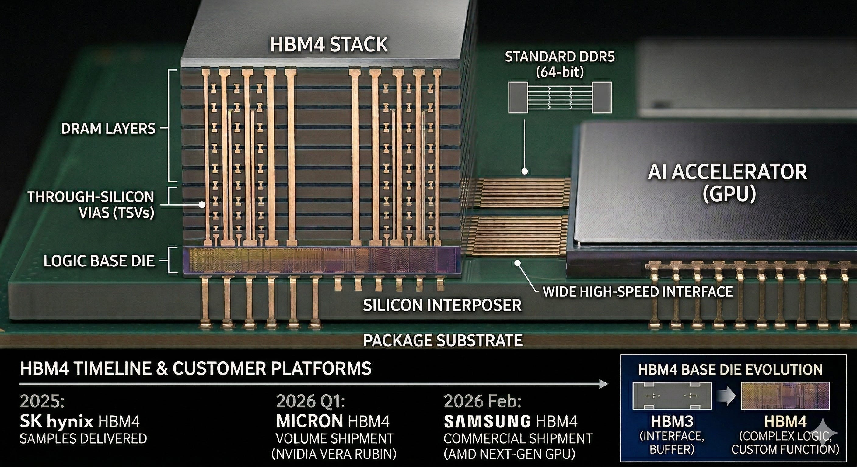
The reason HBM is fast is simple. While standard DDR5 exchanges data with the CPU through a 64-bit-wide bus, HBM uses a far wider interface and much shorter physical paths. The structure is also different. HBM stacks multiple DRAM dies vertically and connects them using TSVs. At the bottom of the stack sits a base die.
Starting with HBM4, the nature of this base die changes. Through HBM3, it primarily handled interface, control, test, and buffering functions. In HBM4, it is evolving to carry more complex logic and customer-specific features. HBM is no longer a product where “just making good memory” is enough. SK hynix has stated it will use TSMC’s advanced logic process for the HBM4 base die. Micron has explained that it is building the HBM4E base logic die in partnership with TSMC. Samsung went a step further and applied a 4nm logic base die.
So where does HBM4 stand right now? Samsung announced commercial shipment of HBM4 in February 2026. Micron stated that it began volume shipment of HBM4 36GB 12H in Q1 2026. SK hynix supplied HBM4 samples to major customers in March 2025 and announced development completion and production readiness in September of the same year. What stands out is that every one of these announcements was tied to a specific customer platform. Samsung’s HBM4 was introduced alongside AMD’s next-generation GPU. Micron’s HBM4 began volume shipment for NVIDIA’s Vera Rubin. SK hynix’s HBM4 was discussed in the context of sample deliveries and qualification with key customers. HBM is not a market where making the chip is the finish line. It is a market where you are only done once the chip is in the customer’s system and running stable.
Why HBM Is So Hard to Make

HBM is everywhere in the conversation right now. Stock forums, news outlets, casual dinner tables — everyone’s heard that “HBM is in short supply” or “NVIDIA can’t build enough GPUs because of HBM.”
CXMT’s HBM: How Far Along, and Where Are the Bottlenecks?
CXMT has set 2026 as its target for HBM3 mass production.
According to Reuters, initial monthly HBM wafer output of around 30,000 wafers has been discussed, and an HBM back-end fab in Shanghai is also in the works. There have been reports of HBM samples being supplied to Huawei, though nothing has been officially confirmed.
YMTC's moves are also worth watching here. YMTC (Yangtze Memory Technologies) is China's leading 3D NAND flash manufacturer, known for its proprietary Xtacking architecture. YMTC established a DRAM subsidiary in September 2025 with registered capital of 20.7 billion yuan (roughly $2.9 billion), and has been reported to be pursuing joint HBM development with CXMT. Given that YMTC's Xtacking-based hybrid bonding capabilities could be applied to HBM packaging, China appears to be preparing for HBM self-sufficiency not through CXMT alone but through a collaborative structure with YMTC. This signals that China's intent to supply HBM domestically, beyond commodity DRAM, is strong.
However, these numbers do not automatically translate into a competitive production setup. In HBM, what matters far more than the date production begins is production yield, package quality, and customer system qualification. Specifically, the bottlenecks CXMT needs to clear are TSV yield, die bonding, and thermal management.
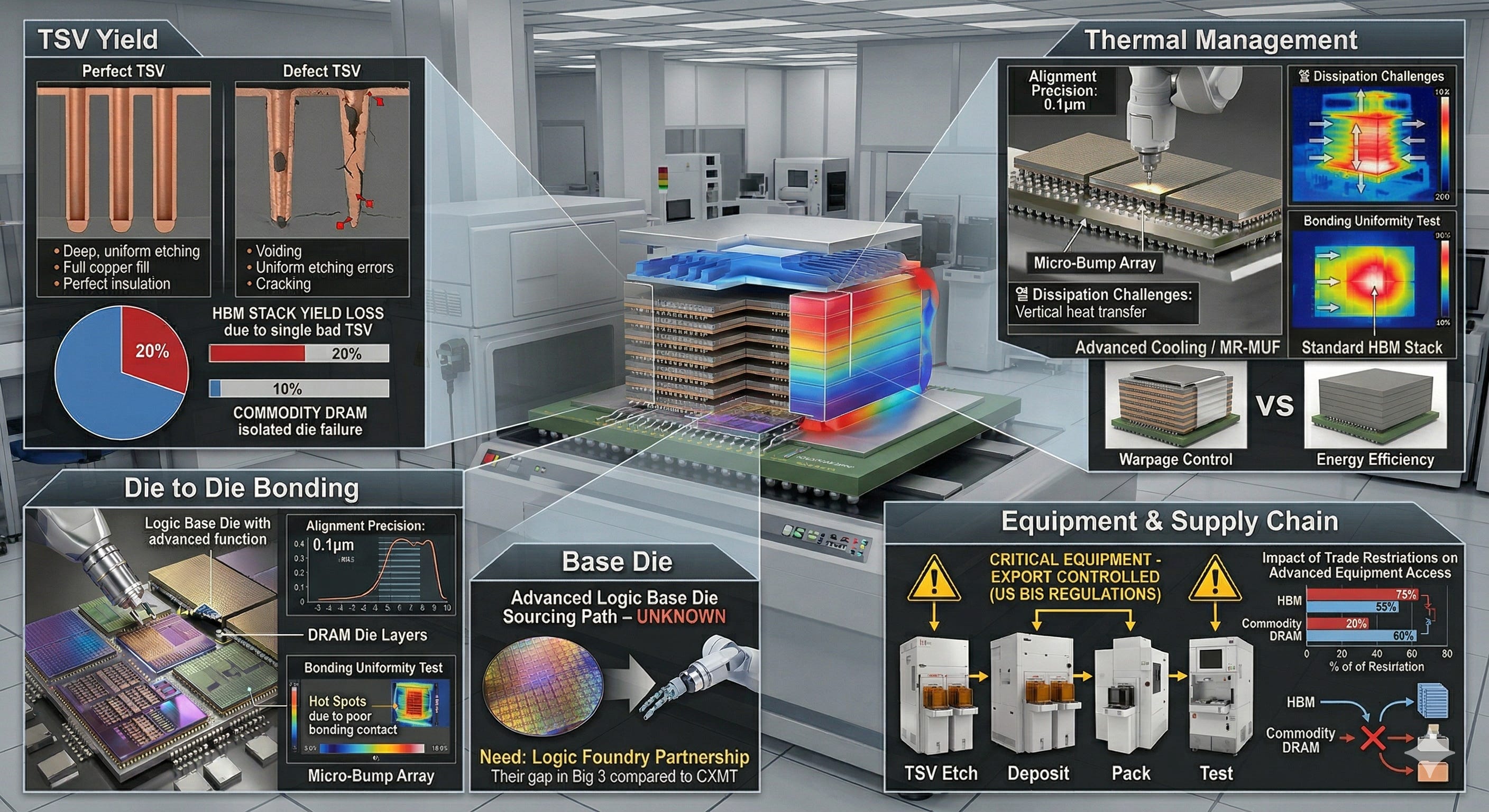
TSV yield. HBM requires stacking multiple DRAM dies vertically, so the stability of the TSV process directly determines stacking yield. Etching deep and uniform holes through silicon, depositing insulation layers, and filling them completely with copper without voids are all steps where a single failure causes problems. Because HBM operates as a single stack of multiple dies, a defect in any one layer can bring down the yield of the entire stack. A defect that might be a single-die issue in commodity DRAM escalates to a total stack value loss in HBM.
Die-to-die bonding. HBM requires electrically connecting multiple stacked dies, and the mainstream approach for HBM3 production is micro bump based. As bump pitch gets tighter, the demands on alignment precision and bonding uniformity go up, and as stack counts increase, a bonding failure in a single layer can destroy the entire stack. For CXMT, stabilizing micro bump bonding at production-grade yield is the challenge it needs to clear first.
Thermal management. Because HBM stacks multiple dies vertically, heat generated in lower layers transfers upward. Temperature increases lead to higher refresh overhead and reliability issues, which ultimately eat into effective performance. The leading companies have spent years accumulating know-how in die thinning, warpage control, thermal interface materials, and package structure optimization. SK hynix highlighted heat dissipation and warpage control through Advanced MR MUF in its HBM4 12-high product, and Samsung also put reliability and energy efficiency front and center in its HBM4 announcement. HBM competitiveness is not determined by circuit design alone. It is determined by comprehensive capability that includes packaging and thermal process experience.
Base die. I explained earlier that the HBM4 base die is evolving toward logic. For CXMT, this becomes an additional barrier. The Big 3 have already secured collaboration paths with advanced logic foundries like TSMC, but in CXMT’s disclosed plans, while HBM3 production and the Shanghai back-end investment are confirmed, an advanced logic base die sourcing path has not yet surfaced. As the industry moves into the HBM4 generation, CXMT will need to solve not just DRAM stacking but logic base die sourcing as well.
Equipment and supply chain. The US BIS, in its December 2024 rule tightening, specifically strengthened controls on HBM and advanced semiconductor manufacturing equipment. The harder China pushes to catch up in HBM, the more constraints it faces across etch, deposition, packaging, and inspection equipment. Chinese equipment makers are trying to develop substitutes, and that is true. But in a market like HBM where stacking, thermal management, bonding, and testing are all intertwined, equipment performance and production stability translate directly into competitiveness.
HBM: Overall Assessment
There is no reason to deny the possibility that CXMT enters HBM3. Given China’s resource mobilization capability, reaching the level of “making HBM3” is likely. But as we have seen, this is a market where TSV yield, die bonding, thermal management, base die sourcing, and equipment constraints are all stacked on top of each other. It is not a matter of solving one. All five need to be stabilized simultaneously at production grade. Reuters, citing TechInsights analysis, reported that CXMT trails SK hynix by up to four years. That gap is not simply a matter of time. It is the accumulation of these bottlenecks.
And the bigger problem is that the leaders are not standing still. By the time CXMT enters HBM3, the Big 3 will already be deep into HBM4 commercial shipments and customer-specific competition. Every time the pursuer completes one generation, the leaders have already moved on to the next.
That does not mean CXMT’s HBM is meaningless. But its value lies in geopolitical supply chain self-sufficiency, not in global leadership competition. US export controls have placed structural constraints on the Chinese AI ecosystem’s access to cutting-edge HBM. In this context, even an HBM3 that trails on performance holds strategic value if it can be reliably sourced within China. CXMT’s HBM is less a card that threatens SK hynix or Samsung in the global market, and more a card that closes the Chinese AI supply chain into a system that is “not cutting-edge, but self-sufficient.”
3D DRAM, Where the Game Gets Flipped
In commodity DRAM and HBM, the Big 3 lead and CXMT chases. But 3D DRAM is different. This is not a game where a latecomer catches up to the leaders. It is closer to a zone where the rules of competition themselves change.
Why 3D DRAM Is Needed
The most basic way to improve DRAM performance has always been shrinking the cell. But that shrink is now approaching physical limits.
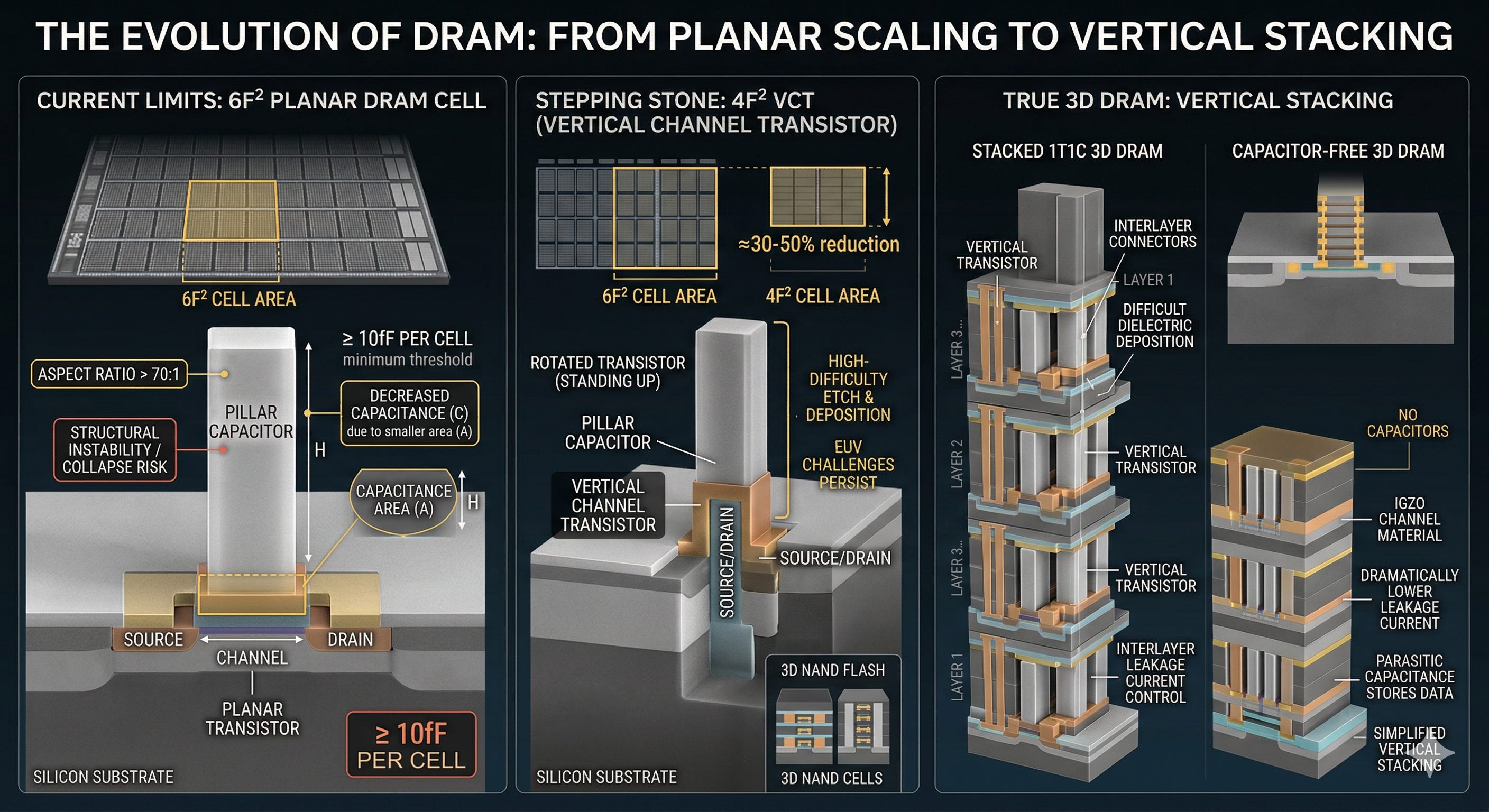
The heart of a DRAM cell is the capacitor. A capacitor consists of two electrode plates with a dielectric, a material that does not conduct electricity, sandwiched between them. As cells get smaller, the electrode area of the capacitor shrinks with them, and the amount of charge it can store, its capacitance, decreases. If the charge gets too small, it becomes impossible to reliably distinguish between 0 and 1. The industry generally considers around 10 femtofarads per cell the minimum threshold.
To address this, the industry has been making capacitors thinner and taller. As the electrode area shrank, height was increased to maintain sidewall surface area. The aspect ratio of capacitors in today’s most advanced DRAM is estimated to exceed ratios of several tens to one, reaching the 70:1 range. A structure one unit wide and 70 or more units tall is an extremely narrow, elongated pillar, and at these proportions the risk of structural collapse or tilting grows significantly. The implication is clear: we are approaching structural limits.
The current industry standard is the 6F² cell layout. Here, F refers to the minimum feature size achievable by the process, and 6F² means each cell occupies an area of 6F² on the wafer surface. Inside that area sits one transistor and one capacitor. The transistor lies horizontally on the wafer surface, and the capacitor stands vertically on top.
4F² VCT: A Stepping Stone to 3D DRAM
Shrinking further requires moving to a 4F² cell. The 4F² cell uses a VCT, or Vertical Channel Transistor, structure. In the conventional 6F² cell, the three parts of the transistor (source, channel, and drain) are laid out side by side on the wafer surface. The source is where current enters, the drain is where it exits, and the channel is the pathway between them. In VCT, this structure is rotated 90 degrees and stood upright. Current flows vertically instead of horizontally.
Why does standing it up save area? A horizontal transistor uses wafer surface space along the direction from source to drain, proportional to channel length. Standing it up moves the channel into the vertical dimension, reducing the footprint on the wafer surface. Going from 6F² to 4F² increases cell density by roughly 30 to 50 percent.
SK hynix has publicly stated it is evaluating a transition to a 4F² VG platform. Both Samsung and SK hynix are developing 4F² prototypes, and the industry expects several more years before volume production. However, 4F² is not a simple shortcut that merely eases the lithography burden. It requires high-difficulty etch and deposition processes to create vertical structures, and EUV challenges persist. Ultimately, 4F² is less a convenient alternative to shrinking and more the first structural step toward 3D DRAM.
Micron is reportedly taking a different path. Industry observers interpret Micron as potentially skipping the 4F² VCT stage and pursuing a more direct route to 3D DRAM.
True 3D DRAM: The Era of Vertical Stacking
If 4F² VCT is about standing up the transistor inside the existing cell, 3D DRAM is about stacking entire cells layer by layer.
This concept is easiest to grasp if you think of 3D NAND first. NAND is the storage memory used in SSDs. 3D NAND stacks storage cells vertically to increase capacity, with YMTC producing 200-plus layers and SK hynix announcing a 321-layer product. 3D DRAM follows the same basic idea: stack DRAM cells vertically to circumvent the limits of planar scaling.
The catch is that DRAM cells are structurally far more complex than NAND cells. NAND uses a charge trap structure to store data. Electrons are trapped inside an insulating layer, making the structure relatively simple. DRAM requires a capacitor, and trying to stack capacitors in 3D causes a cascade of technical challenges. Depositing dielectrics uniformly is difficult, interlayer leakage current must be suppressed, and each layer’s electrical characteristics must remain consistent.
So the industry is exploring two main paths.
The first is 3D DRAM with capacitors retained. This maintains the existing 1T1C structure while going vertical. Samsung has been the most aggressive on this front. It presented research results including internal chip images at the 2023 VLSI Symposium and also opened a dedicated 3D DRAM R&D lab in Silicon Valley.
The second is capacitor-free 3D DRAM. As the name implies, data is stored using only transistors, without capacitors. The key material here is IGZO. IGZO is a type of oxide semiconductor, and transistors made from this material have dramatically lower leakage current than silicon transistors. Leakage current is the tiny amount of current that flows even when a transistor is off. When leakage current is low enough, the transistor’s own parasitic capacitance can hold data for a useful period of time without a separate capacitor. In other words, the capacitor could potentially be eliminated. Without capacitors, the cell structure becomes much simpler, and vertical stacking becomes far easier. SK hynix is openly pursuing research on IGZO channel materials.
Why China Could Find Favorable Ground in 3D DRAM
I mentioned earlier the conversation with the head of SK hynix’s Americas operation at a technology seminar. What he said was specifically about 3D DRAM. He said that in 3D DRAM, China is already ahead of SK hynix, and that hynix is working hard to catch up. For someone who had always assumed Korean memory technology was inherently ahead of China’s, that was a pretty striking thing to hear. So why would he say that?
China’s 3D DRAM technology buildup is already advancing on both the industry and academic fronts simultaneously. CXMT presented a compact DRAM architecture at IEDM 2023 that combined a junctionless GAA vertical channel transistor with a hexagonal capacitor for next-generation 4F² DRAM. It is too early to call this a commercial 3D DRAM product, but the fact that a Chinese DRAM company directly presented a next-generation 4F² structure at a major public conference is not insignificant. CXMT has since revealed through its IPO filings that it plans to direct capital toward advanced DRAM R&D, production line upgrades, and HBM expansion. In other words, China is not simply chasing current DRAM. It is preparing for the next generation of memory architecture at the same time.
The academic side is also notable. A paper published in Science Advances in 2025 by a Chinese research team demonstrated an 8×8 3D stacked IGZO 2T0C DRAM array, achieving 3-bit multi-bit storage and retention exceeding 100 seconds at the array level, all without capacitors. This is not a conceptual proposal. It means the capacitorless structure and monolithic stacking approach, both considered key candidates for 3D DRAM, have been pushed to actual array-level demonstration. China has not yet delivered a finished commercial product, but in the core cell structures and stacking directions for next-generation 3D DRAM, it has clearly established its presence.
The Big 3, on the other hand, are not slow because they lack the technology. Samsung showcased a 16Gb 4F² VCT-based hybrid bonded DRAM at ISSCC 2026, and SK hynix acknowledged at IEEE VLSI 2025 that current DRAM scaling is hitting its limits, stating it would apply 4F² VG and 3D DRAM below the 10nm class. The leading companies know exactly why 3D DRAM is necessary. But for them, the money right now still comes from 2D scaled DRAM and HBM. So 3D DRAM is something they must prepare for, but it is not yet at the very top of their business priorities. For China, the situation is different. In the conventional planar DRAM scaling race, it is stuck perpetually chasing from behind. That makes the incentive to bet far more aggressively on 3D DRAM, where the rules of the game change, significantly greater. That asymmetry is most likely what the Americas head was pointing to.
And structurally, 3D DRAM could be a relatively favorable battlefield for China. Until now, DRAM competition has been a race to shrink the cell smaller, and in that game, the Big 3 with EUV access and deep planar scaling experience held an overwhelming edge. But in 3D DRAM, the center of competition shifts from pure lithography to stacking, hybrid bonding, high-aspect-ratio etch, and vertical structure integration. Both Lam Research and TechInsights see the future competition as no longer about “who can shrink smaller” but about “who can stack, bond, and validate better.”
This is where China has stronger assets than you might expect. YMTC has already been mass-producing 3D NAND based on Xtacking, and according to TrendForce, it leads Samsung and SK hynix in hybrid bonding-related patents. There have even been reports suggesting that Samsung could leverage YMTC-related hybrid bonding patents for its 400-plus-layer NAND. What this means is that China is not starting from scratch when it comes to the stacking, bonding, and vertical integration manufacturing instincts that 3D DRAM will require. In planar DRAM, it was a pursuer trailing by five or more years. But in 3D DRAM, the starting line itself could be partially reset. That is why people say 3D DRAM is the first battlefield where China has a real chance to change the rules of the memory game.
What 3D DRAM Changes: Not Just CXMT, but the Entire Equipment Ecosystem
As we saw earlier, the center of competition in 3D DRAM shifts from lithography to stacking, hybrid bonding, and HAR etch. So the next question is this: in that transition, who actually makes money, and who ends up structurally disadvantaged?
The current 2D DRAM scaling regime is built on top of the equipment order established by American, European, and Japanese companies. ASML holds a monopoly on EUV lithography, Lam Research dominates etch, Applied Materials and Tokyo Electron lead deposition, and KLA commands inspection. The Big 3’s advanced DRAM production is difficult to sustain without this supply chain. But in 3D DRAM, the critical processes change. And in each of those changing processes, Chinese equipment companies are rising.
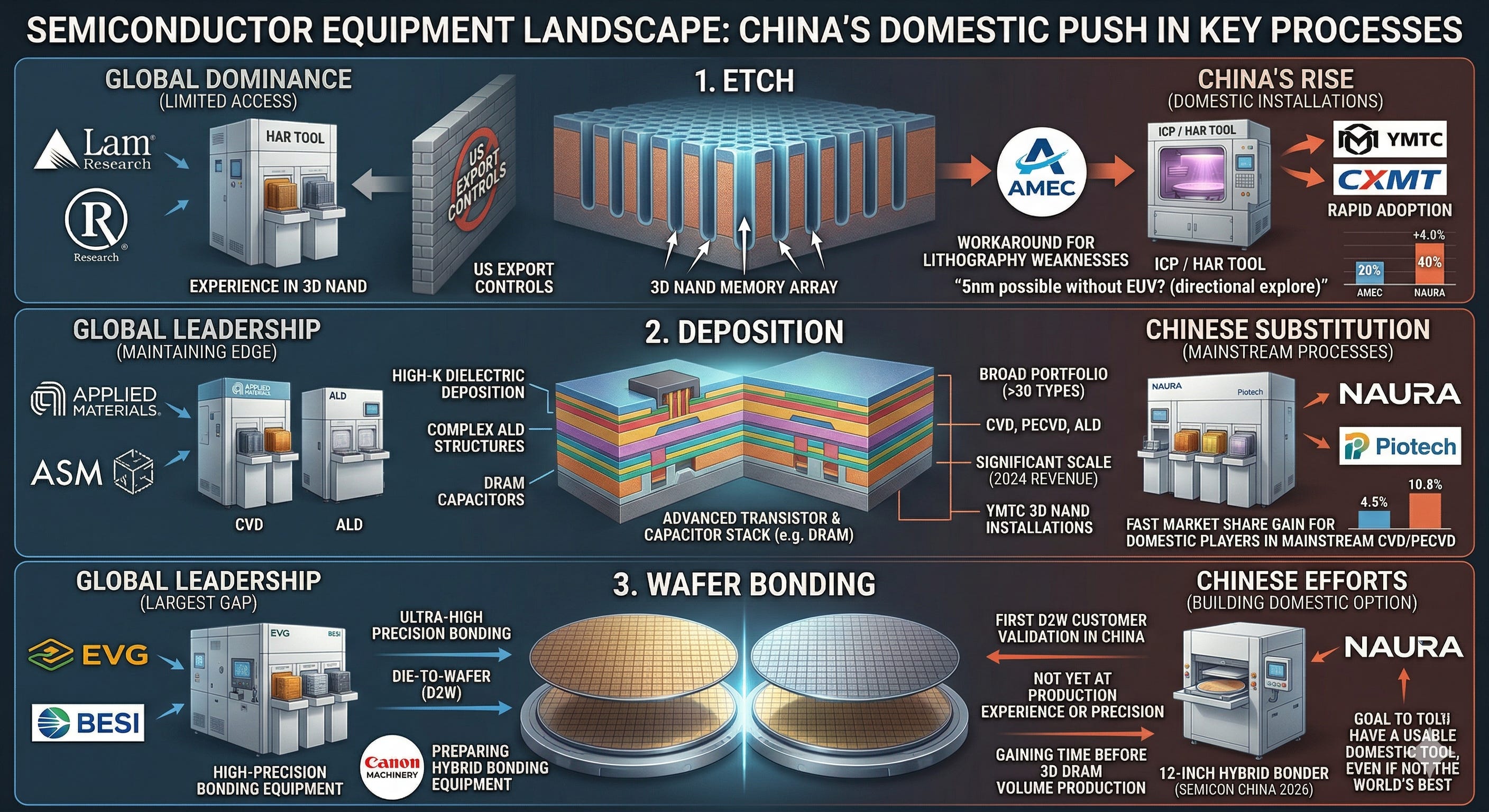
The shift is most visible in etch. In 3D structures, you need to drill deep, narrow channels uniformly through dozens of layers or more. The undisputed global leader in this space is Lam Research. But in China, AMEC is rapidly building its presence. AMEC’s ICP and HAR plasma etch tools are reported to already be installed in YMTC and CXMT production lines. Reporting indicates that in the Chinese etch equipment market, the combined share of AMEC and NAURA has already crossed 40%. While US restrictions limit Lam’s access to China, Chinese companies are filling that void in real terms.
A similar pattern is emerging in deposition. Applied Materials has the strongest presence in CVD and ALD, and it remains unmatched in high-k dielectric deposition for DRAM capacitors. ASM International, as an ALD specialist, is also expected to benefit as structures grow more complex. But in China, NAURA is rising quickly with a portfolio spanning CVD, ALD, and PECVD, and Piotech is expanding its PECVD installation footprint in YMTC’s 3D NAND lines. In advanced new-material deposition like high-k and IGZO, Applied Materials still has a clear edge. But in mainstream CVD and PECVD, substitution within the Chinese domestic market is already moving fast.
Wafer bonding is where the gap between Chinese and global players is largest of the three. In CBA architectures, the cell array wafer and peripheral circuit wafer are fabricated separately and then bonded with high precision. EVG is the global leader, and BESI has strengths in die-to-wafer bonding. In China, NAURA unveiled a 12-inch hybrid bonding tool at SEMICON China 2026 and announced the completion of D2W customer validation, but it has no volume production track record yet. That said, there are still several years before 3D DRAM volume production begins in earnest, and access to global equipment in China is likely to become even harder during that window. What matters in that structure is not the best tool in the world but a tool above a certain threshold that can actually be used domestically.
As I mentioned in the introduction, the ASML employee I spoke with was not taking China’s 3D DRAM lightly either. The reason is clear. If 3D DRAM takes hold, EUV dependency could decline, and the side pushing that transition most aggressively is China, which cannot use EUV in the first place. For ASML, the premise behind memory-driven growth is shaking, and the direction of that shift favors China. This is not a story about ASML collapsing. Logic chips still need EUV, and the High NA transition is on the roadmap. But the premise behind memory-driven growth becomes less straightforward than it used to be. Based on the conversations I have had, my impression is that ASML internally is taking this scenario quite seriously.
Layer the regulatory variable on top and the picture gets even clearer. The MATCH Act introduced in the US Congress in April 2026 aims to restrict the sale and servicing of ASML’s DUV immersion tools to China. It is still at the bill stage, but if China is cut off even more aggressively from advanced lithography access, 3D DRAM stops being just a technical option and becomes effectively the only detour available once the scaling path is blocked. And the critical equipment for that detour is not EUV. It is etch, deposition, and bonding.
Reporting citing China Semiconductor Industry Association data shows that the domestic share of semiconductor equipment in China is rising quickly, with etch and deposition already above 40%. The government has set targets to push that ratio even higher. There is an important caveat: this scenario requires 3D DRAM to actually work in a way that meaningfully reduces EUV dependency. But even the possibility alone could completely reshape which equipment companies benefit and which take the hit.
So what does this mean for Samsung, SK hynix, and Micron?
What Actually Changes for the Big 3
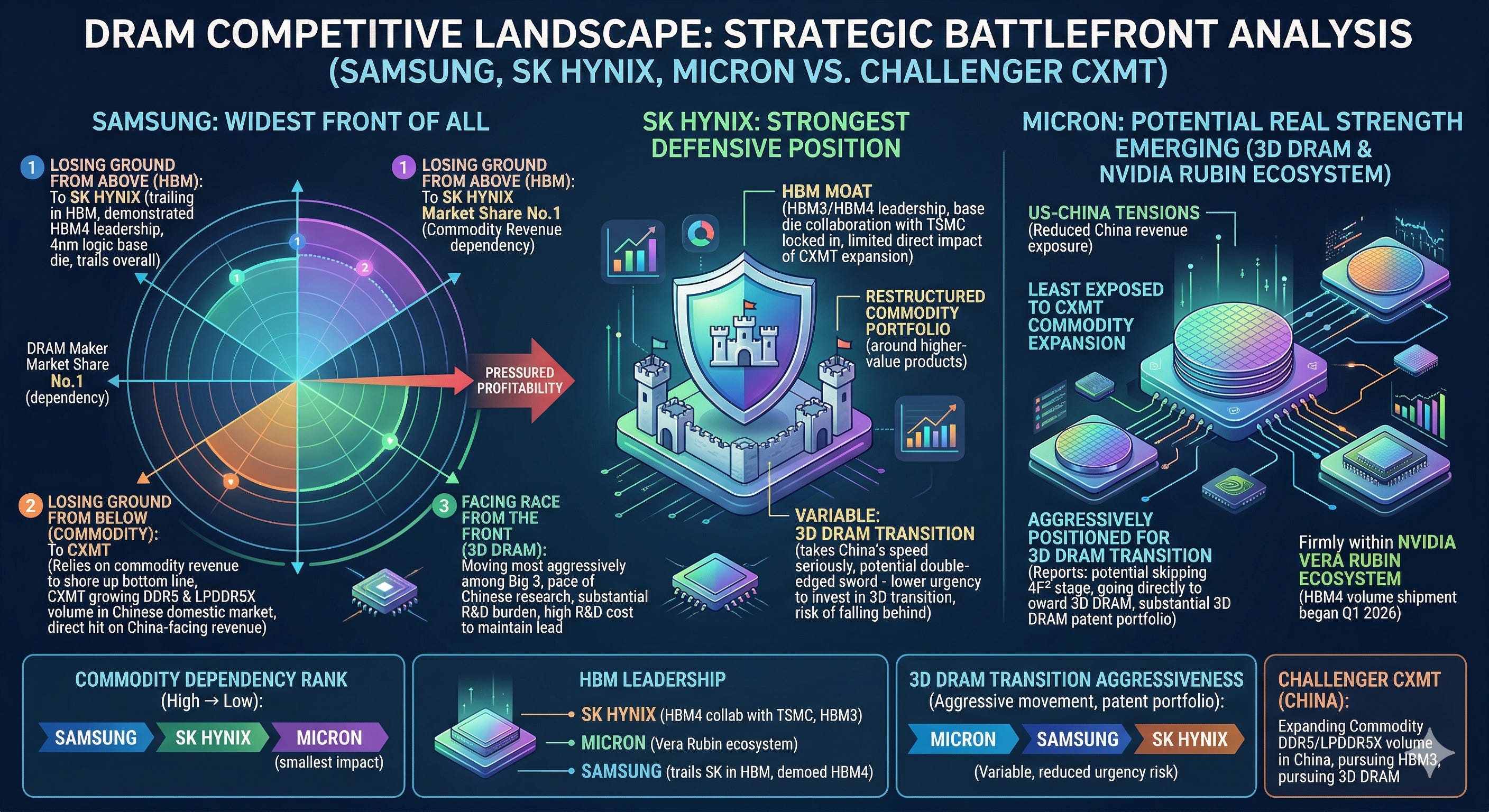
For Samsung, CXMT is the opponent it faces across the widest front.
Samsung is the No. 1 DRAM maker by market share, but it trails SK hynix in HBM and relies on commodity revenue to shore up the bottom line. If CXMT grows DDR5 and LPDDR5X volume in the Chinese domestic market, Samsung’s China-facing commodity revenue takes a direct hit. In HBM4, Samsung has demonstrated technology leadership by applying a 4nm logic base die, but if it gives up ground on the commodity side to CXMT, the profitability of its overall portfolio comes under pressure. In 3D DRAM, Samsung is moving the most aggressively among the Big 3, but given the pace of Chinese research, the R&D burden of maintaining the lead is substantial. Factor in the equipment ecosystem transition, and Samsung is fighting on the widest front of all: losing HBM ground to SK hynix from above, commodity ground to CXMT from below, and facing a 3D DRAM R&D race from the front.
SK hynix has the strongest defensive position for now, thanks to HBM.
Even if CXMT produces HBM3, SK hynix is already competing at the HBM4 level with base die collaboration with TSMC locked in. It has also restructured its commodity portfolio around higher-value products, so the direct impact of CXMT’s commodity expansion is more limited for SK hynix than for Samsung. The variable is the 3D DRAM transition. As the Americas head’s remarks suggest, SK hynix itself takes the speed of China’s pursuit seriously in this area. The stronger the HBM moat, the lower the perceived urgency to invest in the 3D DRAM transition, and that could become a double-edged sword over the long run.
Micron is where the real strength could emerge during the 3D DRAM transition rather than in commodity.
US-China tensions have already reduced Micron’s China revenue exposure, and the direct impact of CXMT’s commodity expansion is the smallest of the three. The reported strategy of potentially skipping the 4F² stage and going more directly toward 3D DRAM, combined with what is known to be a substantial 3D DRAM patent portfolio among the Big 3, could become a source of long-term competitive advantage. Micron’s HBM4 volume shipment also began in Q1 2026, putting it firmly within the NVIDIA Vera Rubin ecosystem. Among the three, Micron is the least exposed to CXMT’s commodity expansion and the most aggressively positioned for the 3D DRAM transition.
Threat or Illusion
In my experience, disruption in the semiconductor industry does not happen when technology catches up incrementally. It happens when the rules of competition change.
SK hynix did not take the initiative from Samsung in the memory market by being better at the same process. It did so by shaping the playing field first in a new game called HBM.
The volume CXMT is already building in commodity DRAM is the result of catching up. But the reason it could become a threat in 3D DRAM is not catching up. It is that the game itself is changing. If you fail to distinguish between these two dynamics, you will misread CXMT.
What to watch going forward is clear. If the CXMT IPO goes through, revenue and yield figures will be disclosed for the first time, exposing the gap between expectations and reality.
If even one of HP, Dell, Acer, or Asus starts putting CXMT memory into actual shipments in DDR5, the commodity story moves beyond the Chinese domestic market.
Whether HBM3 actually makes it into the Huawei Ascend becomes a tangible indicator of China’s AI supply chain self-sufficiency.
On the 3D DRAM side, watch for patent filings and conference publications from CXMT, YMTC, and Chinese research institutes.
On the equipment side, how much of AMEC and NAURA’s tools are actually going into CXMT production lines will reveal the speed of the ecosystem transition.
If two or three of these start moving at the same time, CXMT will no longer be assessed as a “latecomer DRAM maker.” It will be reassessed as a catalyst for structural change in the memory industry.
So memory pricing seems like it will presist until 2028 or so? If 3d RAM becomes viable... China is back in the game and SK goes into tough times again? But this scenario, if at all, won't be true until at least 2030 or so?
Substack needs a comment translate option. Thanks for the nice write up Damnang!