Substrates come up as a bottleneck in almost every recent semiconductor news.
In October, NVIDIA’s Jensen Hwang and, Intel’s Lip-Bu Tan named substrates as a key supply bottleneck.
And it’s not just them.
These days, you can hardly read a semiconductor news story without hearing about substrate bottlenecks.
Okay, so we get it.
But do you know which substrates are we actually talking about?
Semiconductor news uses the word substrate for wafers, interposers, package substrates, motherboards alike, so if you have no engineering background, it is so hard to understand the whole story.
In this article, I’m gonna explain the types of substrates and what they do, then looks at why AI chips use more substrate, why substrate supply cannot be expanded quickly, and why larger substrates yield fewer good units.
It then briefly covers where the supply chain is most blocked, which companies keep the profits, and who secures substrate supply.
I am confident that once you have read it, you will be able to tell for yourself which companies each piece of substrate news favors.
This article is for informational purposes only and does not recommend buying or selling any security. Investors are responsible for their own investment decisions. NFA, DYOR.
What kinds of substrates are there?
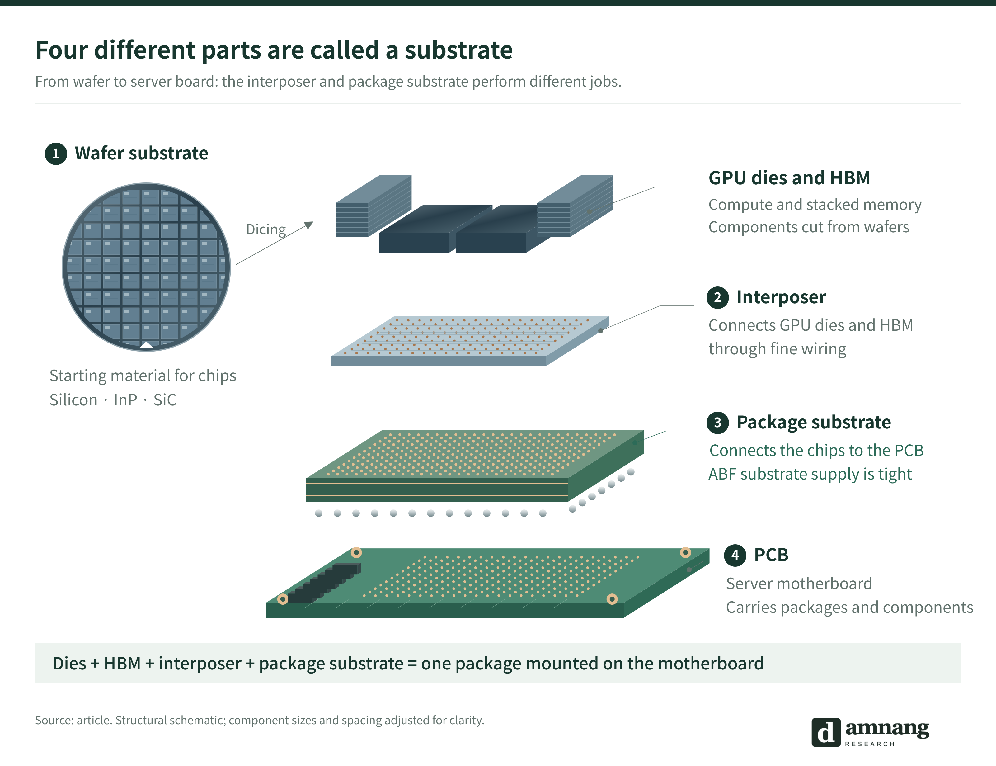
A wafer substrate is the base material chips are built on.
Logic and memory are made on silicon wafers,
many of the lasers in data center optical links on InP (indium phosphide) wafers,
and some high-voltage power semiconductors on SiC (silicon carbide) wafers.
An interposer is a layer that holds GPU dies and HBM, or several GPU dies, side by side and connects them with very fine wiring. Interposers are used because there are too many wires between the chips, packed too closely together.
For example, HBM4 has 2,048 pins just for data connecting with the GPU. Connecting that many pins right next to the GPU takes very fine, dense wiring, so a conventional package substrate cannot easily provide.
Damnang’s Note
TSMC’s CoWoS (chip on wafer on substrate) is built around this interposer.
On the other hand, Intel’s EMIB uses no interposer and buries a small silicon bridge inside the package substrate, only under the spot where two chips meet.
A package substrate is the board that connects a chip or an interposer to the motherboard. The industry also calls the package substrate an IC substrate.
High-performance chips such as CPUs, GPUs and switch chips use ABF substrates, whose insulating layers are made of a film called ABF. Memory and mobile chips mostly use BT substrates, made with BT resin.
Damnang’s Note
ABF substrates are also called FC-BGA substrates because they are used in the FC-BGA (Flip Chip - Ball Grid Array) format.
A PCB (printed circuit board) is a large board, such as a server motherboard, that carries several of these packages along with other components. PCBs and package substrates are both made by stacking copper wiring layers and insulating layers, but the package substrate is much smaller and its wiring is finer and denser.
Of wafers, interposers, package substrates and PCBs, the one in shortest supply today is the ABF package substrate that connects AI chips to the motherboard.
What does an ABF package substrate look like, and what does it do?
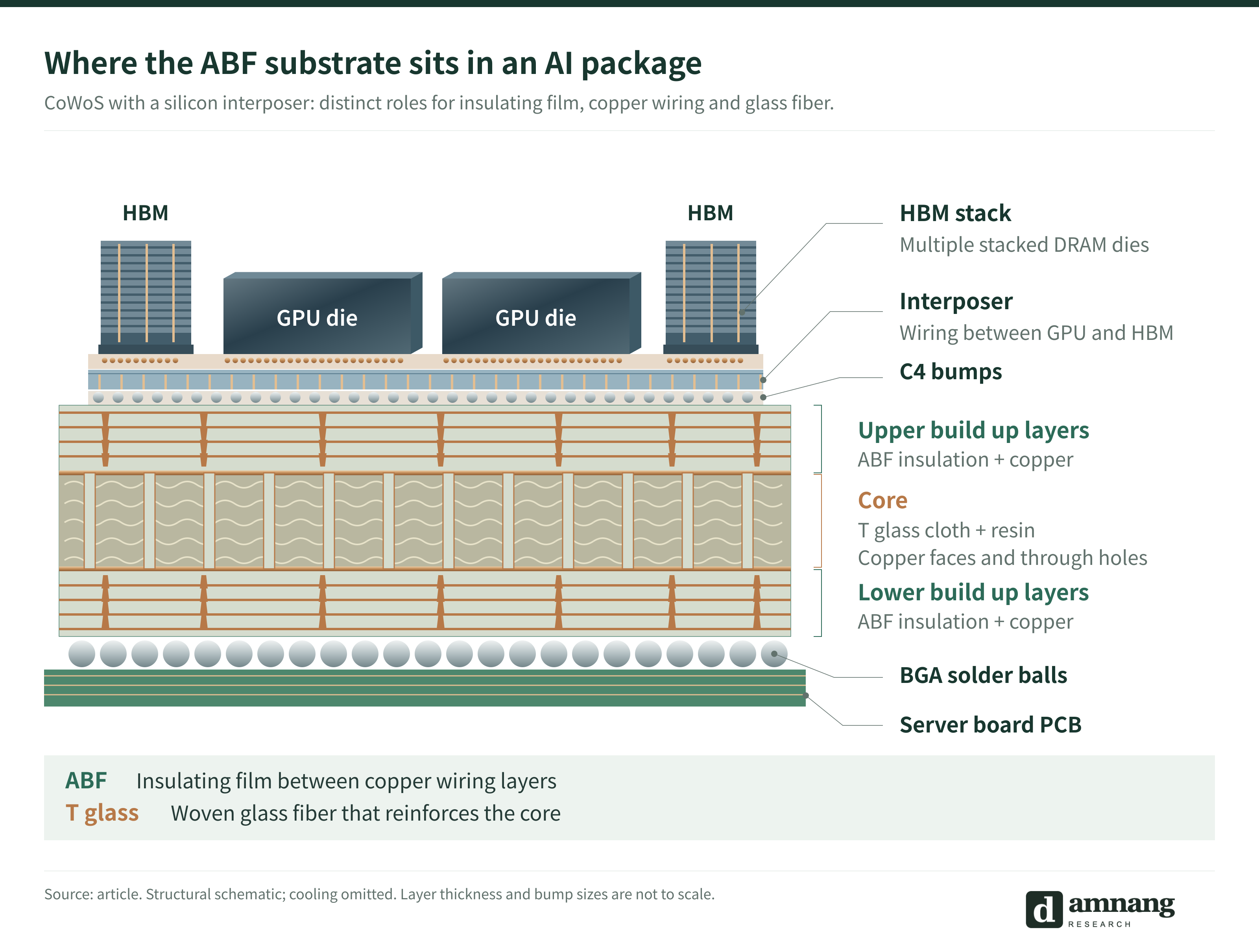
A package substrate consists of a core in the middle and build-up layers stacked above and below it.
The core is made from a copper-clad laminate (CCL), which is glass fiber cloth soaked in resin with copper foil bonded to both sides. Cores for AI chip substrates use T-glass, a premium glass fiber cloth with low thermal expansion. The build-up layers alternate, one layer at a time, between an insulating film called ABF (Ajinomoto Build-up Film) and copper wiring.
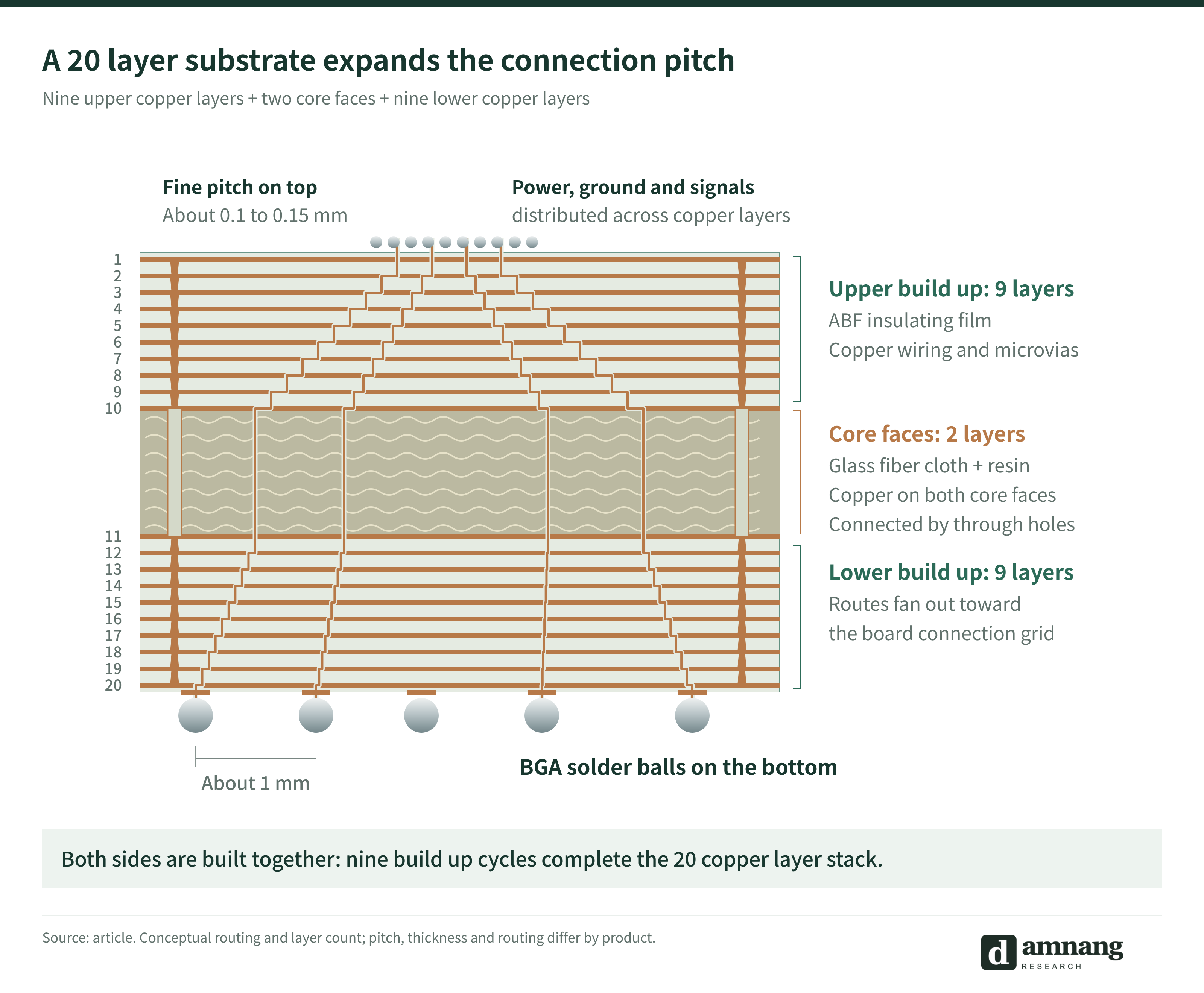
The package substrate widens the spacing of tens of thousands of connections a little at each layer until it matches the motherboard. This is called fan-out. The more connections a chip has, the more layers are needed to carry the wiring.
From here, I’ll take a closer look at why AI chips require more substrate capacity,
where the bottlenecks actually lie,
which parts of the substrate supply chain face the tightest constraints,
and how chipmakers are managing those constraints.